

Field effect transistor construction adopting heavy doped conduction substrate, inverse groove and earthed source pole
A field effect transistor, heavily doped technology, applied in semiconductor devices, electrical components, circuits, etc., can solve the problems of larger package size, larger device size, and increased device cost.
- Summary
- Abstract
- Description
- Claims
- Application Information
AI Technical Summary
Problems solved by technology
Method used
Image

Examples
Embodiment Construction
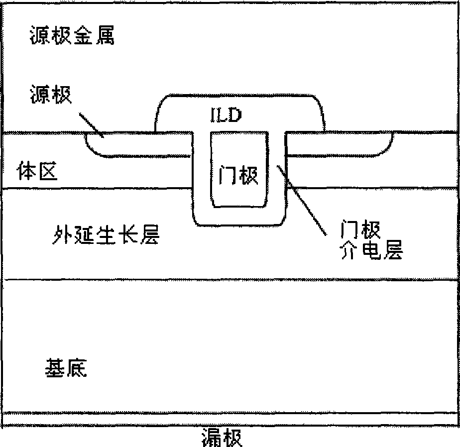
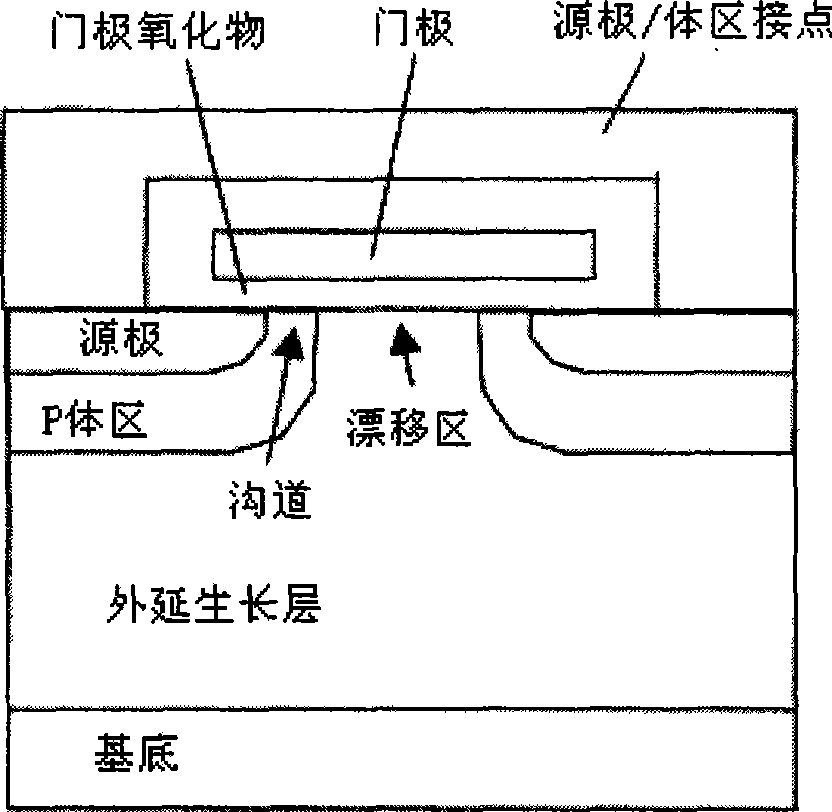
[0023] refer to figure 2A cross-sectional view of an N-channel source-grounded inverted trench FET device with bottom-source-top-drain (ie, source at the bottom and drain at the top) of the present invention. The N-channel inverted trench FET device with its source grounded is supported on a P+ substrate 105 which functions as a bottom source. The alternative is to form P-channel devices on N+ Si substrates, or use silicon carbide, gallium nitride (GaN) or other semiconductor substrates. A P epitaxial growth layer 110 is formed on top of the substrate 105 . The active unit area is configured on the substrate, and the termination area is usually arranged on the periphery of the substrate. The FET device 100 has a plurality of trenches opening on the top surface of the substrate, which reach as deep as the lower portion of the epitaxial growth layer 110 . The trench opened on the active cell area is wider to form a gate, and the sidewall of the trench to which the gate polys...
PUM
 Abstract
Description
Claims
Application Information