Plasma display apparatus
A display device, plasma technology, applied in identification devices, optical/shielding devices, static indicators, etc., can solve the problems of high manufacturing unit price and large number of switching elements, and achieve the effect of reducing manufacturing unit price
- Summary
- Abstract
- Description
- Claims
- Application Information
AI Technical Summary
Problems solved by technology
Method used
Image

Examples
Embodiment Construction
[0018] The specific embodiment of the present invention will be further described below in conjunction with accompanying drawing:
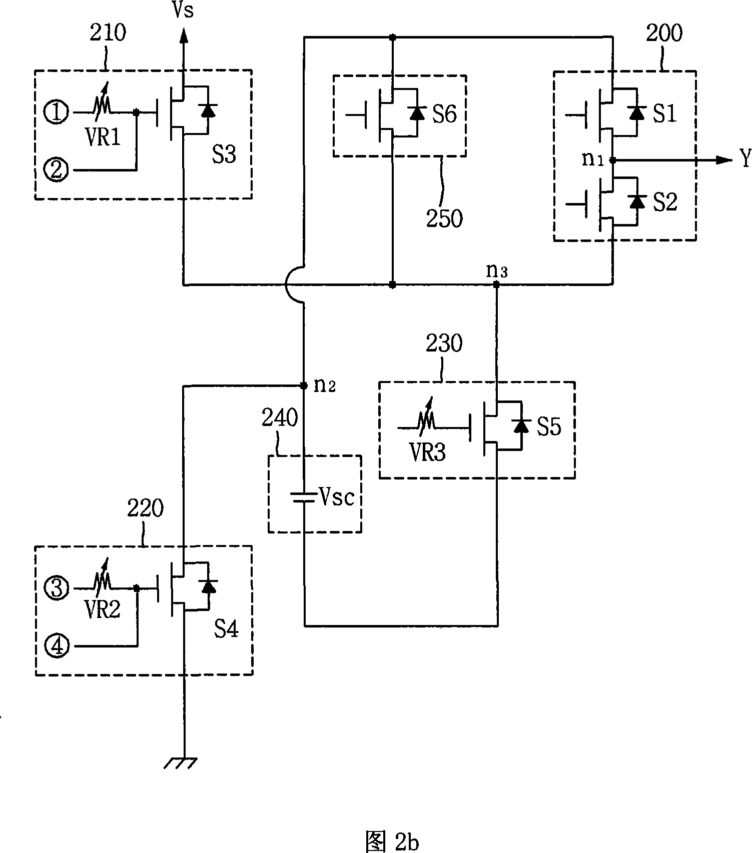
[0019] A plasma display device of the present invention includes a plasma display panel and a drive unit.
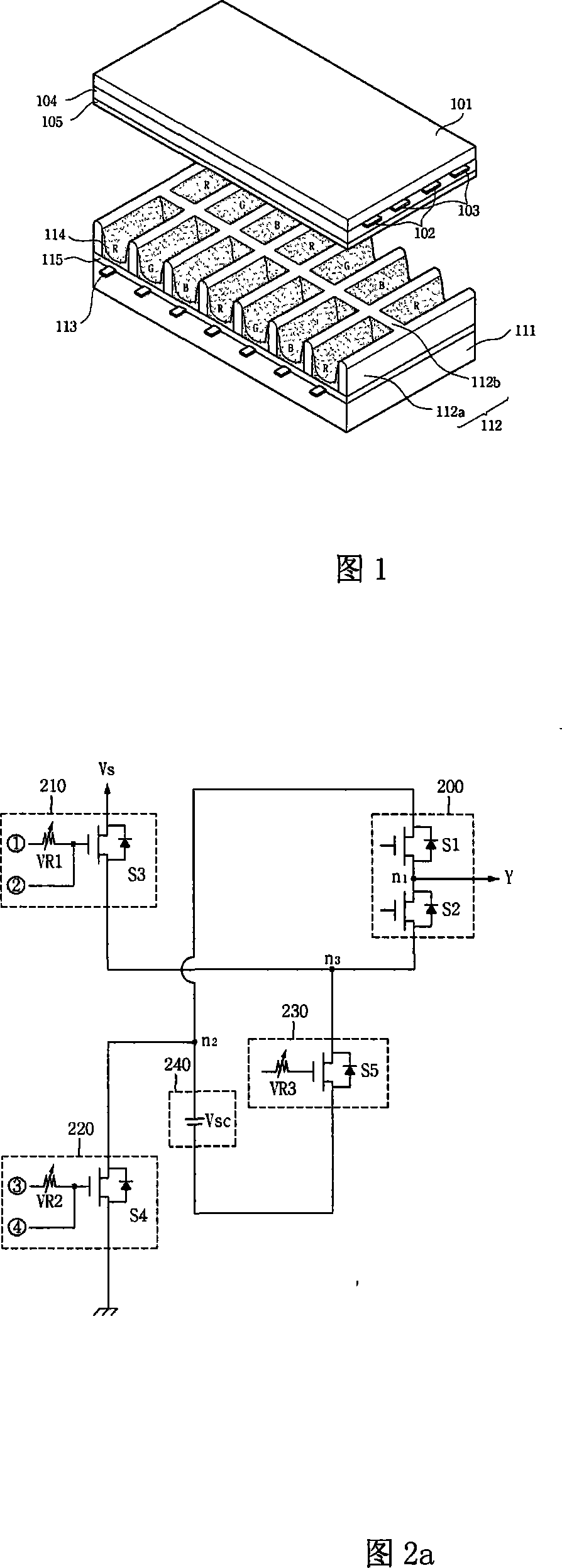
[0020] FIG. 1 is a diagram for introducing a structure of a plasma display panel that may be included in a plasma display device of an example of the present invention.
[0021] Analyzing Fig. 1, then the plasma display panel that can be included in the plasma display device of an example of the present invention is by the front substrate 101 of configuration mutually side by side scan electrode (102, Y) and sustain electrode (103, Z), and front substrate 101 opposite The rear substrate 111 is bonded with the address electrodes 113 intersecting the scan electrodes 102 and the sustain electrodes 103 .
[0022] On the upper portion of front substrate 101 where scan electrodes 102 and sustain electrodes 103 are formed, upper dielectric layer 1...
PUM
 Abstract
Description
Claims
Application Information
 - R&D
- Intellectual Property
- Life Sciences
- Materials
- Tech Scout
- Unparalleled Data Quality
- Higher Quality Content
- 60% Fewer Hallucinations
Browse by: Latest US Patents, China's latest patents, Technical Efficacy Thesaurus, Application Domain, Technology Topic, Popular Technical Reports.
© 2025 PatSnap. All rights reserved.Legal|Privacy policy|Modern Slavery Act Transparency Statement|Sitemap|About US| Contact US: help@patsnap.com