Glue film and chip encapsulation manufacture process using the glue film

A technology of chip packaging and adhesive film, which is applied in the direction of film/sheet adhesives, adhesives, and other chemical processes, and can solve the problems of lowering process yield and inability to maintain the height of the first chip, etc.

Active Publication Date: 2008-06-18
ORIENT SEMICON ELECTRONICS
View PDF0 Cites 8 Cited by
  • Summary
  • Abstract
  • Description
  • Claims
  • Application Information

AI Technical Summary

Problems solved by technology

Although the use of the semi-cured resin can avoid coating each time the die is bonded to shorten the process time, since the semi-cured resin forms a molten state after heating, when the stress of bonding the die ...

Method used


Image

  • Glue film and chip encapsulation manufacture process using the glue film
  • Glue film and chip encapsulation manufacture process using the glue film
  • Glue film and chip encapsulation manufacture process using the glue film

Examples


Embodiment Construction

[0041] In order to make the above and other objects, features and advantages of the present invention more apparent, the following specifically cites the embodiments of the present invention, together with the accompanying drawings, for a detailed description as follows.

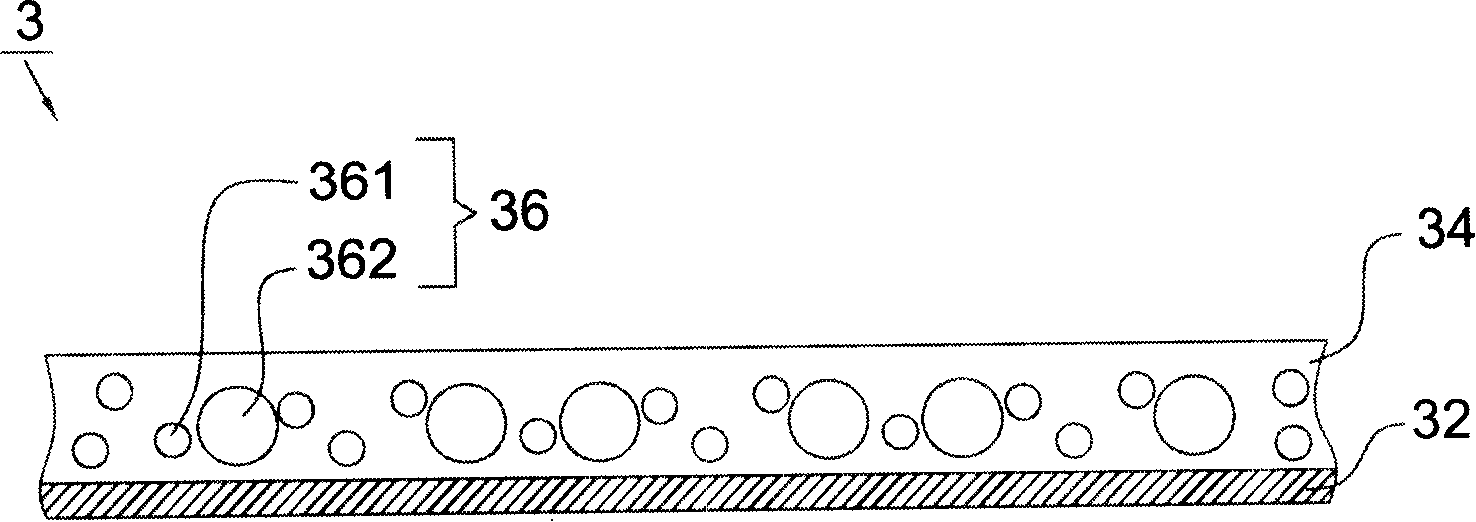
[0042] Such as Figure 3a As shown, the adhesive film (film) 3 of the first embodiment of the present invention is disclosed, which includes a removable base material 32 , a resin layer 34 and a plurality of arc-shaped elastic bodies 36 disposed in the resin layer 34 . The adhesive film 3 is used in the packaging process of the semiconductor chip as an adhesive material for the chip. The embodiment of this substrate 32 can be BT substrate (BT substrate) or adhesive tape (tape); When it is BT substrate, it can utilize epoxy resin (epoxy) to combine with this resin layer 34; When it is adhesive tape, It can be UV tape or blue tape, and it is flexible. The base material 32 is bonded with the resin layer 34 mix...


PUM


Abstract

A glue film comprises removable substrate, a resin layer and a plurality of arc elastic bodies; wherein, the resin layer which is partially curing resin is in a semi-melting status with viscosity above a first temperature and is in solid condition without viscosity under a second temperature, and the resin layer is adhesively arranged on the substrate; the arc elastic bodies are arranged in the resin layer. The invention additionally provides the packaging procedure of a chip using the glue film.

Description

technical field [0001] The invention relates to an adhesive film, in particular to an adhesive film used in a chip packaging process. Background technique [0002] In the package structure of the chip stack that has been used, as shown in FIG. 1 , the package structure includes a substrate 10 , a lower chip 20 , a dummy die 30 and an upper chip 40 . The lower chip 20 is fixed on the substrate 10 by glue 22, and the upper surface of the lower chip 20 is provided with a plurality of aluminum pads 24 on both sides of the upper surface, which are electrically connected by a plurality of first bonding wires 26. Sexually connected to a plurality of pads 12 of the substrate 10 . The dummy chip 30 is fixed on the lower chip 20 by an adhesive 32 and defines a space required by the first bonding wire 26 , for example, a height above about 5 mils (1 mil=25.4 microns). The upper chip 40 is fixed on the dummy chip 30 by glue 42, and the upper surface 48 of the upper chip 40 is provided...

Claims


Application Information

Patent Timeline
IPC IPC(8): H01L23/10H01L23/28H01L23/29H01L23/31H01L23/00H01L21/58H01L21/56H01L21/50C09J7/02C09K3/10
CPCH01L2224/83191H01L2224/48091H01L24/27H01L24/29H01L2224/73265H01L2224/32145H01L24/32H01L2224/83101H01L2224/27436H01L2924/00014
Inventor 董悦明孙国洋杨家铭麦鸿泰刘蕙绮
Owner ORIENT SEMICON ELECTRONICS
Why Eureka
Try Eureka