
Method of programming multi-level cells and non-volatile memory device including the same

A non-volatile storage, multi-layer cell technology, applied in static memory, read-only memory, digital memory information, etc., can solve problems such as complex configuration, and achieve the effect of reducing integration rate and total programming time

Inactive Publication Date: 2008-06-25
SAMSUNG ELECTRONICS CO LTD
View PDF2 Cites 17 Cited by
  • Summary
  • Abstract
  • Description
  • Claims
  • Application Information

AI Technical Summary

Problems solved by technology

[0033] Therefore, traditional non-volatile memory devices require complex configuration

Method used

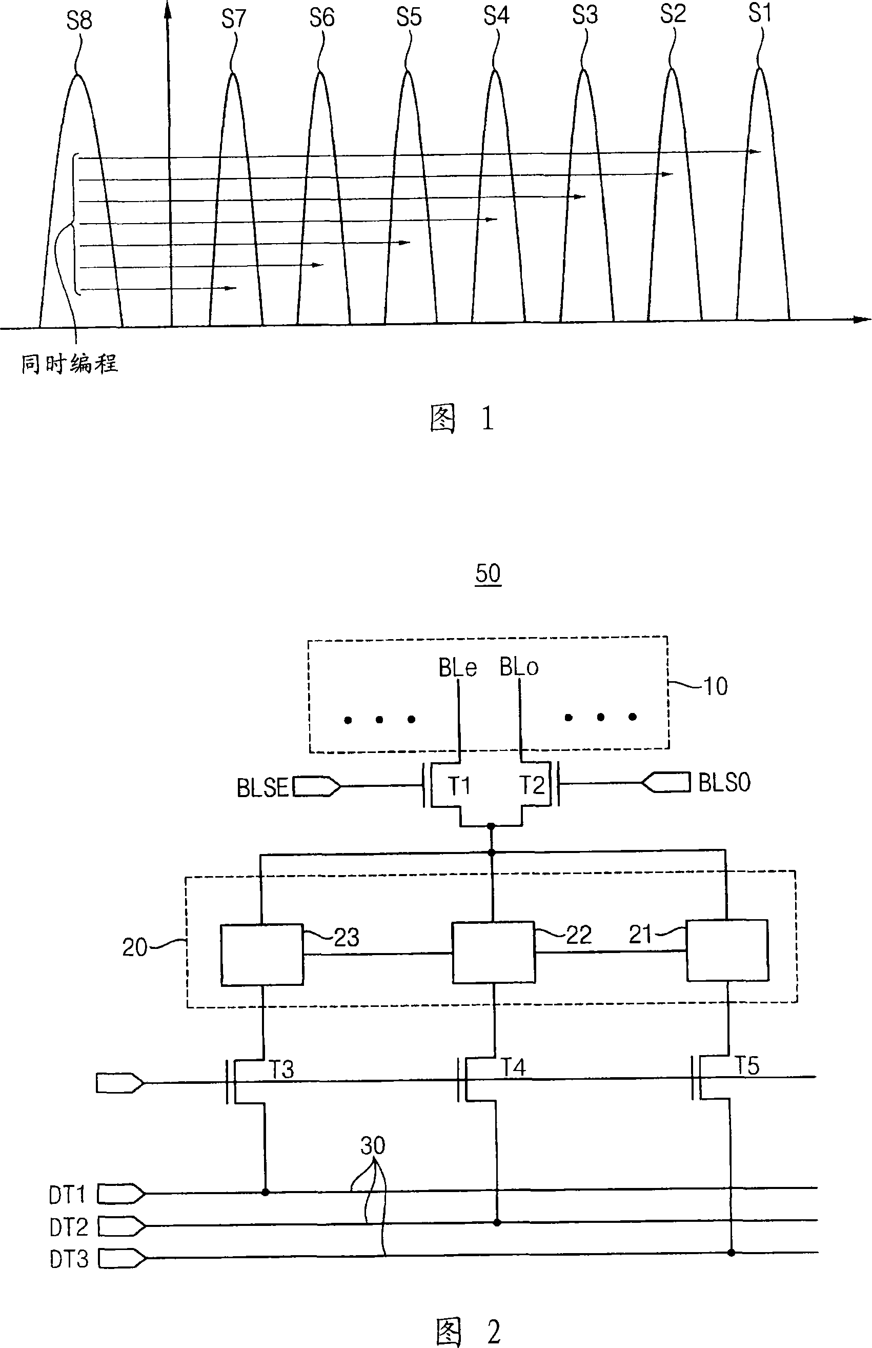
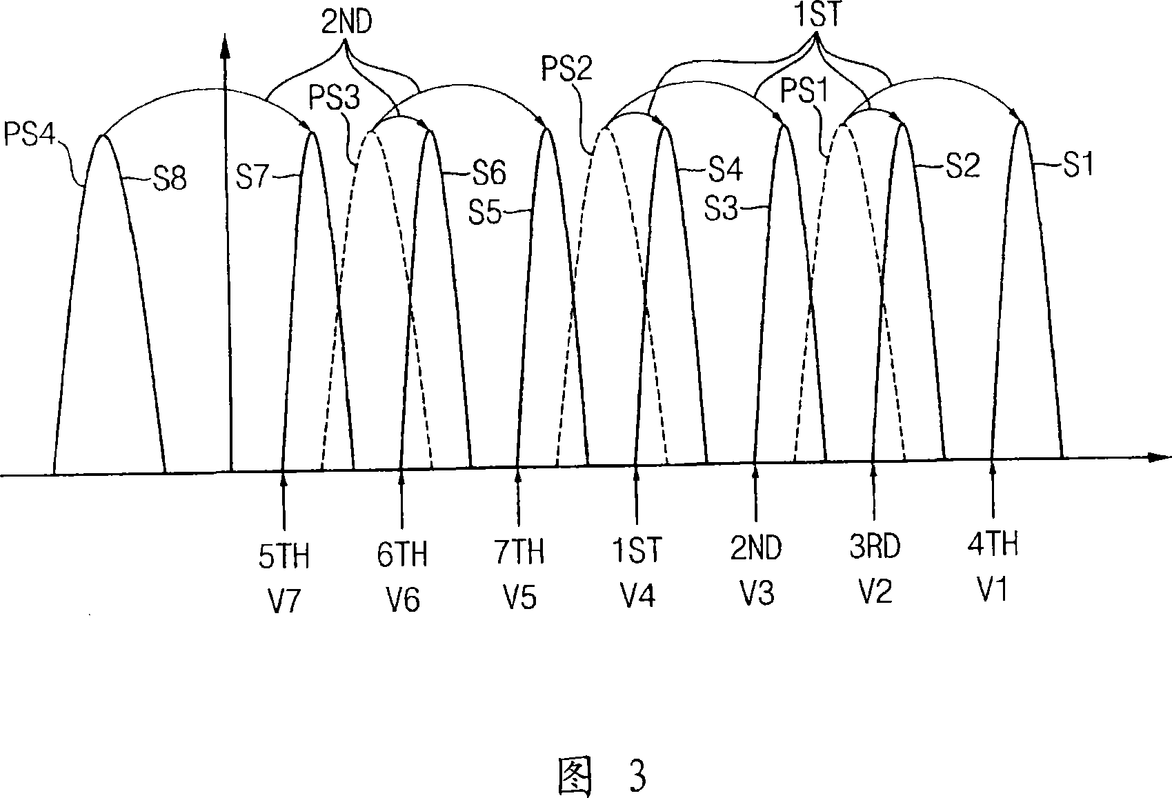
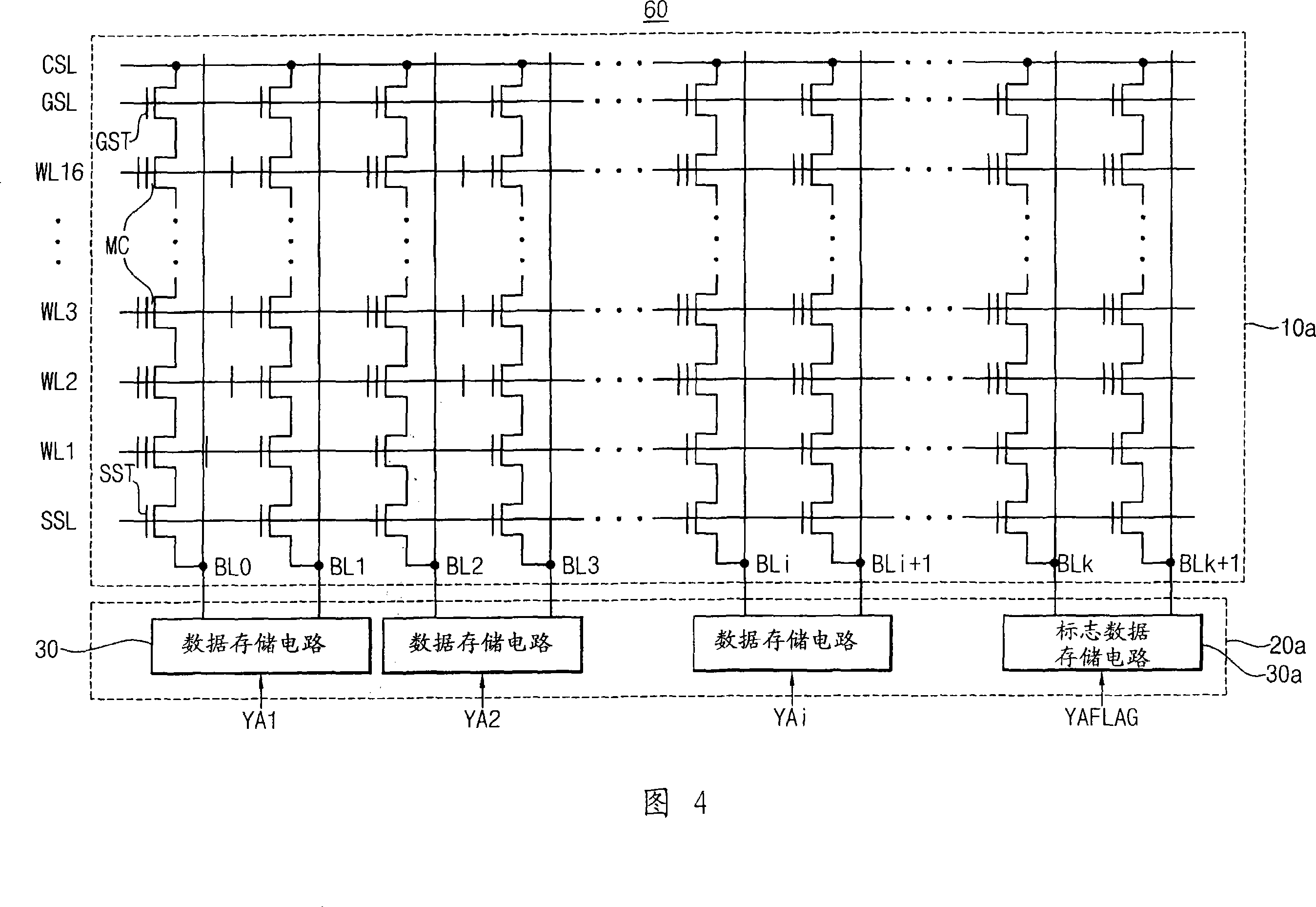

Image

  • Method of programming multi-level cells and non-volatile memory device including the same
  • Method of programming multi-level cells and non-volatile memory device including the same
  • Method of programming multi-level cells and non-volatile memory device including the same

Examples


Embodiment Construction

[0077] Hereinafter, the present invention will be described in more detail with reference to the accompanying drawings showing exemplary embodiments of the invention. This invention may, however, be embodied in various different forms and should not be construed as limited to only the illustrated embodiments. Rather, these embodiments are provided as examples in order to convey the concept of the invention to those skilled in the art. Accordingly, known processes, elements and techniques are not described in connection with some embodiments of the present invention. Throughout the drawings and written description, the same reference numerals are used to refer to the same or similar elements.

[0078] It will be understood that although the terms first, second etc. may be used to describe various elements, these elements should not be limited by these terms. These terms are only used to distinguish one element from another. For example, a first element could be termed a seco...


PUM


Abstract

A non-volatile memory device has multi-level cells (MLCs), which are programmed such that one page is written in the MLCs having previous states corresponding to at least one previous page. The non-volatile memory device includes a memory cell array, a row selection circuit and a page buffer block. The memory cell array includes the MLCs commonly coupled to a selected word line and respectively coupled to bitlines. The row selection circuit applies sequentially-decreasing read voltages to the selected wordline to read the previous states of the MLCs, and sequentially-decreasing verification voltages to the selected wordline to program states of the MLCs sequentially from a state having a highest threshold voltage to a state having a lowest threshold voltage. The page buffer block loads data corresponding to the one page, and controls a bitline voltage based on each previous state and each bit of the loaded data.

Description

[0001] Cross References to Related Applications [0002] This application claims priority from Korean Patent Application No. 10-2006-0127578 filed on December 14, 2006, the subject matter of which is hereby incorporated by reference. technical field [0003] The present invention relates to programming non-volatile memory devices, and more particularly, to methods of programming multi-level cells and non-volatile memories including page buffer blocks pieces. Background technique [0004] Semiconductor memory devices are generally classified into nonvolatile memory devices that retain stored data when power is turned off, and volatile memory devices that lose stored data when power is turned off. Nonvolatile memory devices include electrically erasable programmable read only memory (EEPROM), in which stored data can be electrically erased and reprogrammed with new data. [0005] The operation of EEPROM includes: programming mode, for writing data into the memory cell; read ...

Claims


Application Information

Patent Timeline
Patent Type & Authority Applications(China)
IPC IPC(8): G11C16/10
CPCG11C2216/14G11C16/0483G11C11/5642G11C11/5628G11C16/3459G11C2211/5621G11C16/04G11C16/06G11C16/10G11C16/30
Inventor 朴起台李永宅金奇南金杜坤
Owner SAMSUNG ELECTRONICS CO LTD
Learn More