Supercharge Your Innovation With Domain-Expert AI Agents!

Single layer polysilicon grid OTP device and method for forming the same

A technology of single-layer polysilicon and polysilicon, which is applied in the manufacture of electrical solid-state devices, semiconductor devices, semiconductor/solid-state devices, etc., can solve the problems of large space, inability to effectively reduce the device area, and the large area of ​​a single OTP device, and achieve a small area , large unit capacitance and high coupling efficiency

Active Publication Date: 2012-06-20
SHANGHAI HUAHONG GRACE SEMICON MFG CORP
View PDF0 Cites 0 Cited by
  • Summary
  • Abstract
  • Description
  • Claims
  • Application Information

AI Technical Summary

Problems solved by technology

The problem with this structure is usually that the unit capacitance of the transistor capacitor is small, so the area of ​​a single OTP device is often large; there are also transistor capacitors made into structures such as well capacitors (NWC) to increase the potential area capacitance and improve coupling efficiency, but also Because the space required for well isolation is large, the device area cannot be effectively reduced

Method used


Image

  • Single layer polysilicon grid OTP device and method for forming the same
  • Single layer polysilicon grid OTP device and method for forming the same
  • Single layer polysilicon grid OTP device and method for forming the same

Examples


Embodiment

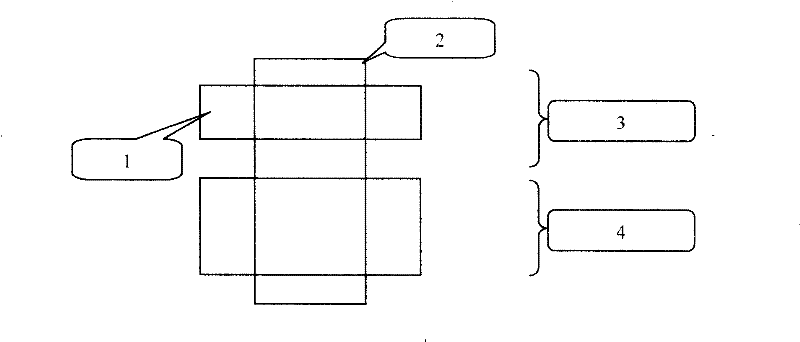
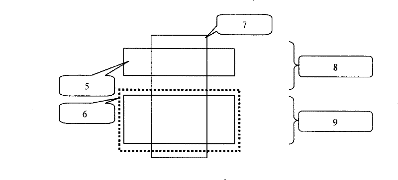
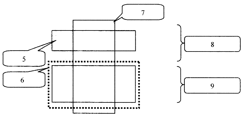
[0014] Such as figure 2 It is the device design and structure of a specific embodiment of the present invention, wherein: 5. Active region, 6. Offset injection region, 7. Polysilicon gate, 8. Memory transistor, 9. Transistor capacitor region. The structure features a high-voltage offset implant in an existing high-voltage process figure 2 The device structure of the buried layer (or similar to the buried layer) is formed on the capacitor side of the transistor shown. With the buried layer, the capacitance value per unit area of ​​the transistor capacitor is improved, and the overall coupling efficiency of the OTP device is increased; at the same time, due to the buried layer The depth of the junction is usually deeper (should be deeper than the common source-drain junction), so this also improves the breakdown voltage of the transistor-capacitance active region junction; therefore, this embodiment effectively realizes embedding with reduced area, good programming effect, and...


PUM


Abstract

The invention discloses a monolayer polysilicon gate OTP apparatus and the forming method thereof. The OTP apparatus comprises a traditional memory transistor (8) and a transistor capacitance section (9), but a pre-buried layer structure (6) is formed at the side of the capacitance of the transistor. To form the apparatus, the excursive injection in the high voltage process is utilized to form the pre-buried layer structure at the side of the capacitance side of the transistor on the basis of the prior high voltage process. The invention utilizes the existing excursive injection in the priorhigh voltage process to form the embedded type OTP technology with large specific capacitance, high coupling efficiency, and small area in the transistor capacitance section on the basis that any process condition is not changed through the design of the apparatus.

Description

technical field [0001] The invention relates to OTP design and manufacturing technology in semiconductor integrated circuits, in particular to a single-layer polysilicon gate OTP device and a forming method thereof. Background technique [0002] With the continuous development of semiconductor integrated circuits (ICs), in many logic circuits and high-voltage process applications (such as LCD-Driver, etc.), one-time programmable memory (OTP, One Time Programmable) devices are often required. Because the required OTP capacity is often relatively small, it is hoped that the effect of embedding OTP can be achieved through device design without changing the existing process. However, the existing single-layer polysilicon OTP (Single Poly OTP) structure basically adopts a similar figure 1 The OTP structure shown generally consists of two parts: a memory transistor and a transistor capacitor region, wherein: 1. Active region, 2. Polysilicon gate, 3. Memory transistor, 4. Transist...

Claims


Application Information

Patent Timeline
Patent Type & Authority Patents(China)
IPC IPC(8): H01L27/115H01L21/8247H01L21/04
Inventor 徐向明龚顺强
Owner SHANGHAI HUAHONG GRACE SEMICON MFG CORP
Features
  • R&D
  • Intellectual Property
  • Life Sciences
  • Materials
  • Tech Scout
  • Unparalleled Data Quality
  • Higher Quality Content
  • 60% Fewer Hallucinations
Learn More