Sheet adhering apparatus

A chip sticking device and chip technology, applied to adhesives, electrical components, circuits, etc., can solve the problems of chip waste, inappropriateness, and easily broken chips, and achieve the effect of precise pasting and avoiding waste

Active Publication Date: 2008-07-02
LINTEC CORP
View PDF1 Cites 3 Cited by
  • Summary
  • Abstract
  • Description
  • Claims
  • Application Information

AI Technical Summary

Problems solved by technology

Therefore, in an extremely thin plate-shaped member that is ground into a wafer, which is only tens of microns, if a thin sheet leaving traces of recesses is used, the thickness will be uneven, and the wafer will be easily broken during grinding, so the recessed area cannot be used as a chip. paste chip
Therefore, although it is sufficient to convey the sheet so as not to include the above-mentioned concave region, it is not suitable because the sheet will be consumed for no reason.
[0006] Such an unreasonable phenomenon can be solved by setting the guide rollers 28 groups at positions very close to the outer edge of the wafer, but it cannot correspond to the occasion of changing the size of the table according to the size of the wafer. The waste of flakes cannot be avoided
[0007] In addition, the above-mentioned unsuitable phenomenon caused by the traces of the rib-like recesses also occurs when the peeling sheet is used.

Method used


Image

  • Sheet adhering apparatus
  • Sheet adhering apparatus
  • Sheet adhering apparatus

Examples


Embodiment Construction

[0031] Hereinafter, embodiments of the present invention will be described with reference to the drawings.

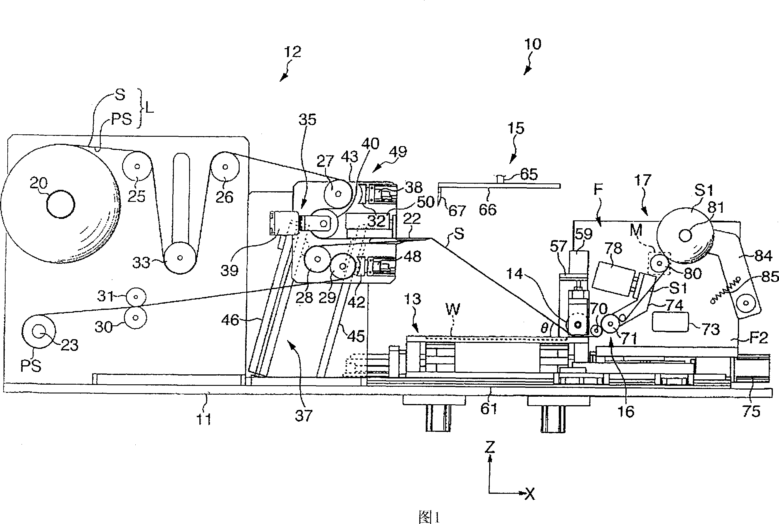
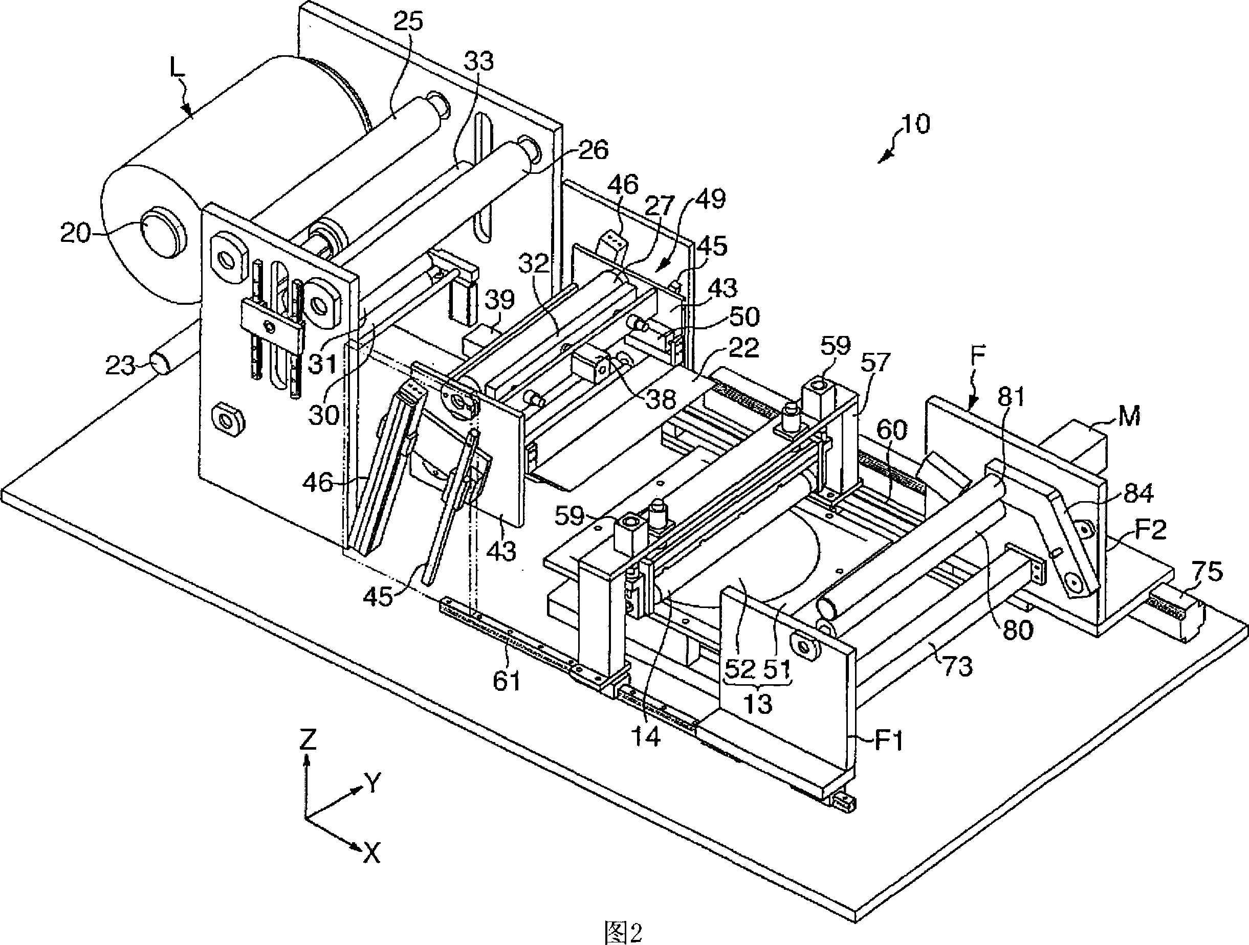
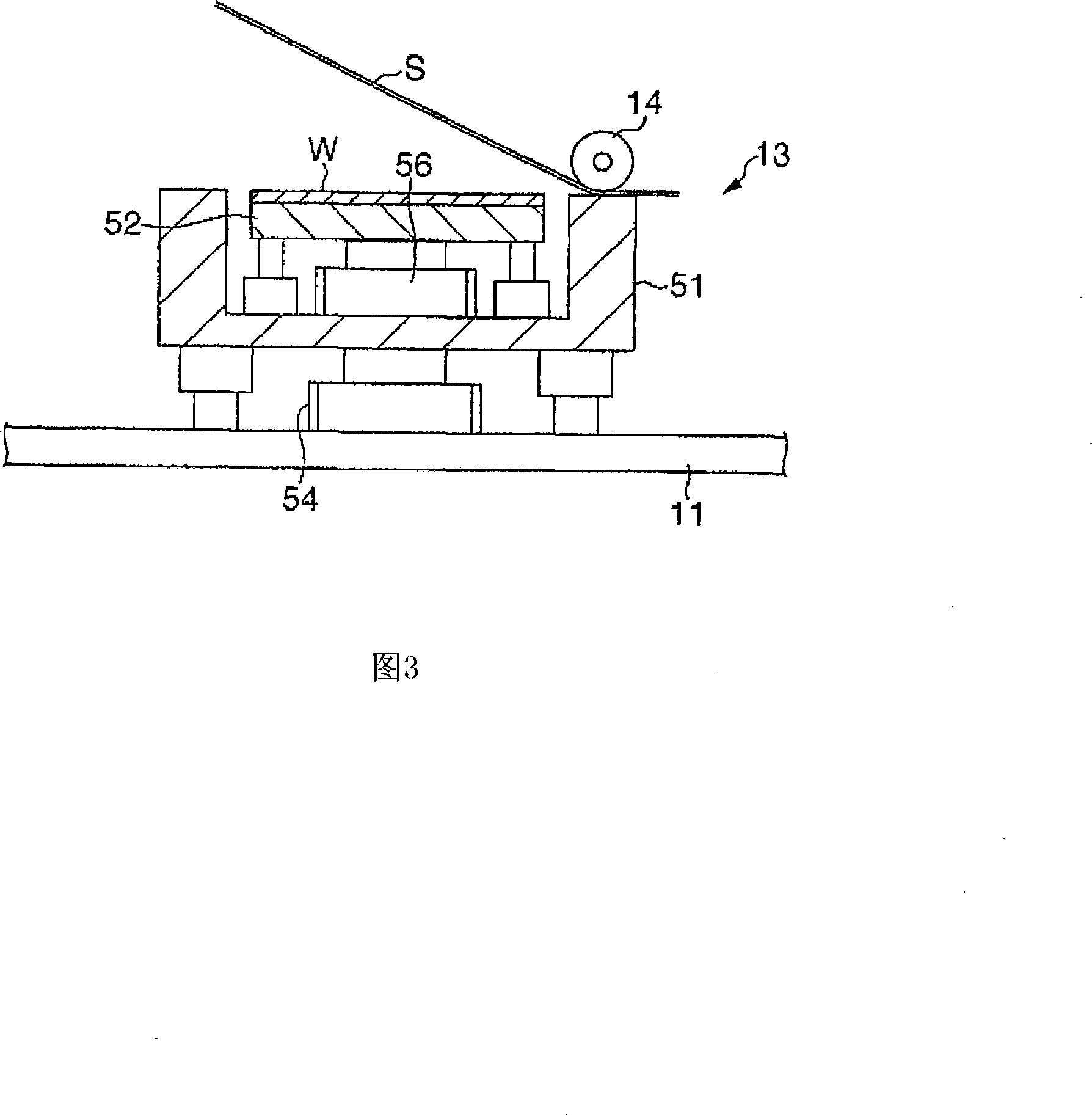
[0032] FIG. 1 shows a schematic front view of the sheet sticking device according to this embodiment, and FIG. 2 shows a schematic perspective view thereof. In these figures, the sheet sticking apparatus 10 is composed of the following components: a sheet guide unit 12 arranged on the upper part of the base 11; a table 13 supporting a wafer W as a plate-shaped member; The pressure roller 14 that sticks the adhesive sheet S on the upper side to the wafer W by applying a pressing force; and the cutter 15 that cuts the adhesive sheet S along the outer edge of the wafer W after the adhesive sheet S is attached to the wafer W; and a peeling device 16 for peeling the unnecessary adhesive sheet S1 on the outer side of the wafer W from the upper surface of the table 13; and a take-up device 17 for winding the unnecessary adhesive sheet S1.

[0033] The above-mentioned sheet gu...


PUM


Abstract

A sheet adhering apparatus is provided with a sheet feeding unit (12) which includes a peel plate (22) for peeling an adhesive sheet (S) from a peeling sheet (PS), and a pressing roller (14) for pressing and adhering the adhesive sheet (S) to the wafer (W) supported by a table (13). The peel plate (22) is supported to move forward and backward by means of a cylinder (50). The initial position of the leading end of the peel plate (22) is adjusted to the front and rear in accordance with the size of the wafer (W) or the size of the table which supports the wafer (W).

Description

technical field [0001] The present invention relates to a sheet sticking device, and more specifically, to a sheet sticking device which can prevent the waste of the sheet when sticking the chip to a plate-shaped member such as a semiconductor wafer. Background technique [0002] Traditionally, on a semiconductor wafer (hereinafter referred to as "wafer"), a protective sheet for protecting the circuit surface is generally pasted, or an adhesive sheet for chip soldering is pasted on the back thereof. [0003] There is known such a sheet sticking device (for example, refer to Patent Document 1): use a kind of roll paper (raw material sheet) that is temporarily stuck with a tape-shaped adhesive sheet on a tape-shaped release sheet, After the tab is peeled and attached to the wafer, it is cut along the periphery of the wafer. [0004] Patent Document 1 Japanese Patent Laid-Open No. 2004-47976 [0005] However, in the sheet bonding apparatus disclosed in Patent Document 1, sinc...

Claims


Application Information

Patent Timeline
Patent Type & Authority Applications(China)
IPC IPC(8): H01L21/683
CPCY10T156/1343Y10T156/17Y10T156/1705H01L21/67132H01L21/683
Inventor 野中英明小林贤治
Owner LINTEC CORP
Why Eureka
Try Eureka