A chip table top etching device

A technology of mesa corrosion and chips, applied in the direction of electrical components, semiconductor/solid-state device manufacturing, circuits, etc., can solve the problems of long time and complicated process procedures, and achieve the effect of simple operation, simplified process and simplified operation process.

Active Publication Date: 2008-07-09
ZHUZHOU CRRC TIMES SEMICON CO LTD
View PDF0 Cites 7 Cited by
  • Summary
  • Abstract
  • Description
  • Claims
  • Application Information

AI Technical Summary

Problems solved by technology

[0005] The problem solved by the present invention is to overcome th

Method used


Image

  • A chip table top etching device
  • A chip table top etching device
  • A chip table top etching device

Examples


Embodiment Construction

[0034] In order to make the above objects, features and advantages of the present invention more comprehensible, specific implementations of the present invention will be described in detail below in conjunction with the accompanying drawings.

[0035] In the following description, numerous specific details are set forth in order to provide a thorough understanding of the present invention. However, the present invention can be implemented in many ways other than those described here, and those skilled in the art can make similar extensions without departing from the connotation of the present invention. Accordingly, the invention is not limited to the specific implementations disclosed below.

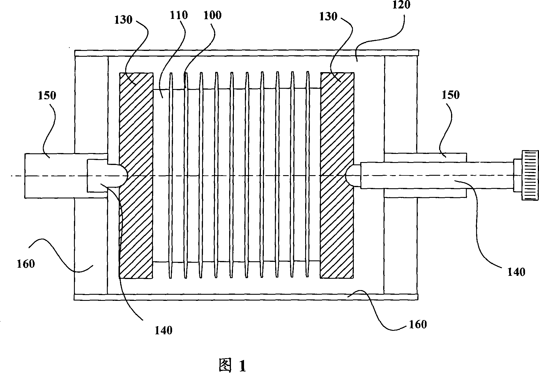
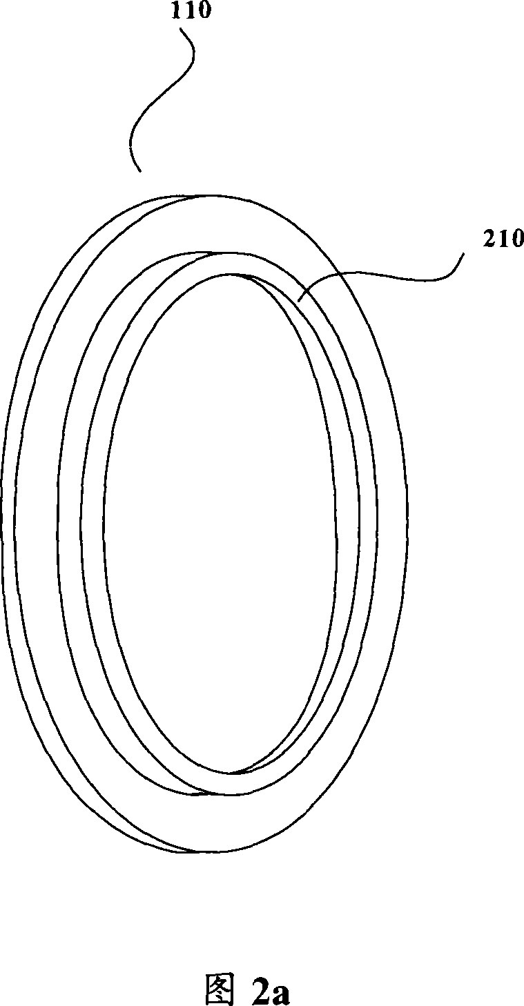
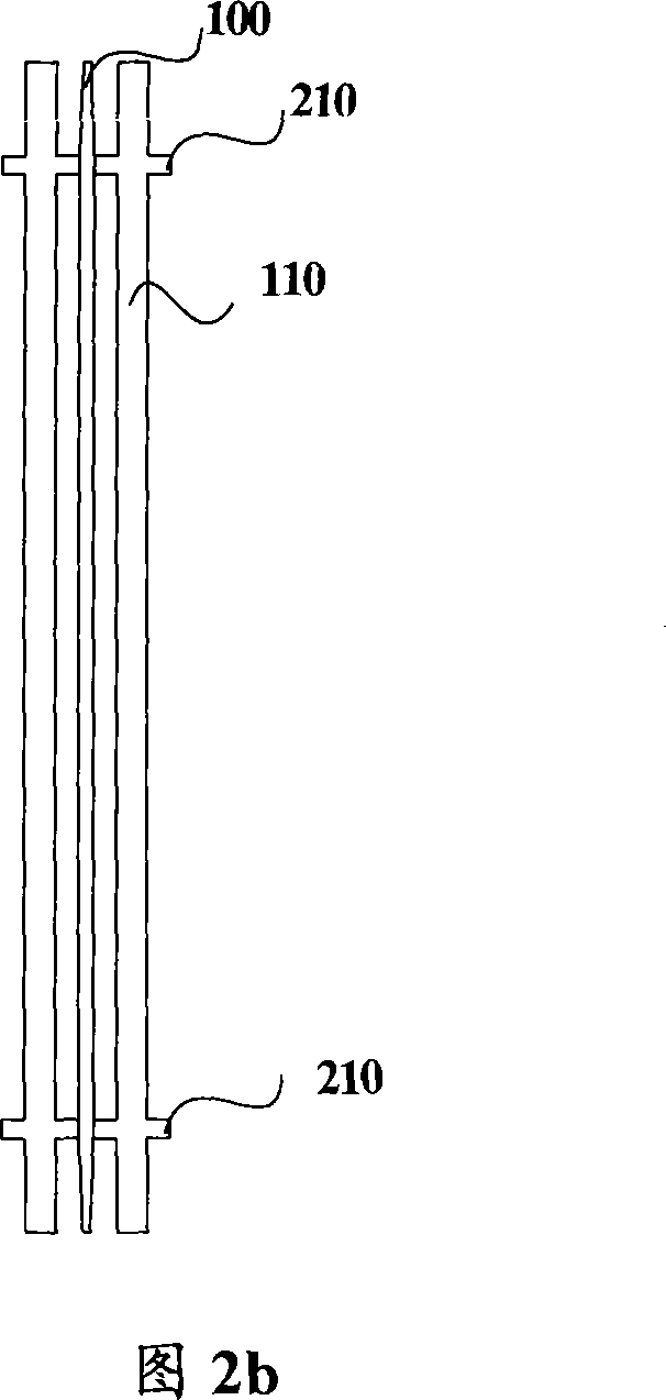
[0036] FIG. 1 is a schematic structural diagram of a chip mesa etching device according to an embodiment of the present invention. As shown in FIG. 1 , the chip mesa etching device includes a spacer 110 and a chip frame 120 . The spacer 110 is circular and made of corrosion-resistant...


PUM


Abstract

The invention discloses a chip mesa etching device, which mainly includes a spacer and a chip frame; the spacer takes a shape of round slice; the chip frame includes baffles, a locking device, a rotation device and a fixed frame; the baffles are positioned at the both sides of the chip frame, the outsides of the baffles are connected with the locking device, the locking device can inwardly extrude the baffles, then the spacer and a chip which are arranged between the baffles can be clamped tightly by the baffles, the rotating device is sheathed at the outside of the locking device, the locking device is embedded and sheathed in the side surface of the fixed frame and is connected with the side surface, the locking device and the rotation device extend to the outside from both sides of the side surface of the fixed frame. The invention eliminates the coating of a chip protective coating layer and solves the problems of complicated process procedure and the long time of the traditional method. Furthermore, the invention has simple operation, can load dozens of chips at one time, as well as carry out the corrosion simultaneously and greatly improve the working efficiency.

Description

technical field [0001] The invention relates to the technical field of semiconductor manufacturing, in particular to a chip mesa etching device. Background technique [0002] With the advancement of power device manufacturing technology and the continuous improvement of market requirements for device capacity, power thyristors and rectifier devices are developing in the direction of high current and high voltage. In order to increase the current capacity of the device, the size of the device must be increased. As the size of the device increases, the stress caused by thermal expansion between materials increases, so that the original sintered structure is no longer suitable for the manufacture of thyristors and rectifier devices of 4 inches and above. Instead, full pressure connection structure. [0003] In sintered structures, the shaping of the device is only done on one side. The fully crimped structure chip has no substrate support, and its shape is generally double-si...

Claims


Application Information

Patent Timeline
IPC IPC(8): H01L21/00H01L21/306
Inventor 黄建伟刘国友邹冰艳李世平潘昭海
Owner ZHUZHOU CRRC TIMES SEMICON CO LTD
Why Eureka
Try Eureka