Method for eliminating CuxO resistance memory formation voltage

A resistance memory and voltage technology, applied in the field of microelectronics, can solve problems such as device performance degradation, no resistance conversion characteristics, and storage medium damage

Inactive Publication Date: 2010-11-17
FUDAN UNIV
View PDF5 Cites 0 Cited by
  • Summary
  • Abstract
  • Description
  • Claims
  • Application Information

AI Technical Summary

Problems solved by technology

CuO does not contribute to the resistive switching characteristics, while for Cu x When the O-based resistive memory is written for the first time, it needs to use a relatively large formation voltage to break down the CuO film on the surface layer. y O storage medium produces damage, leading to device performance degradation

Method used


Image

  • Method for eliminating CuxO resistance memory formation voltage
  • Method for eliminating CuxO resistance memory formation voltage
  • Method for eliminating CuxO resistance memory formation voltage

Examples


Embodiment Construction

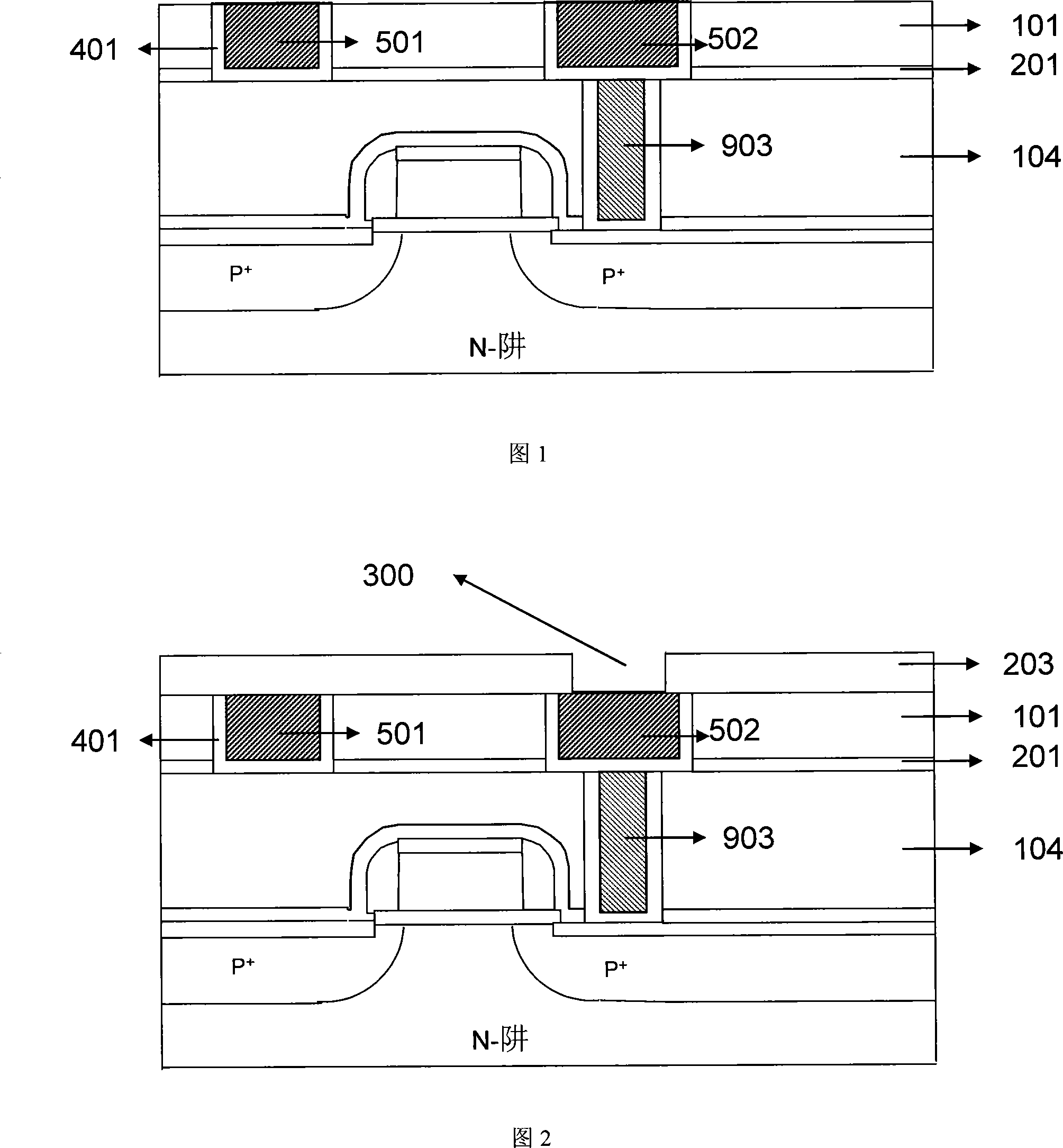
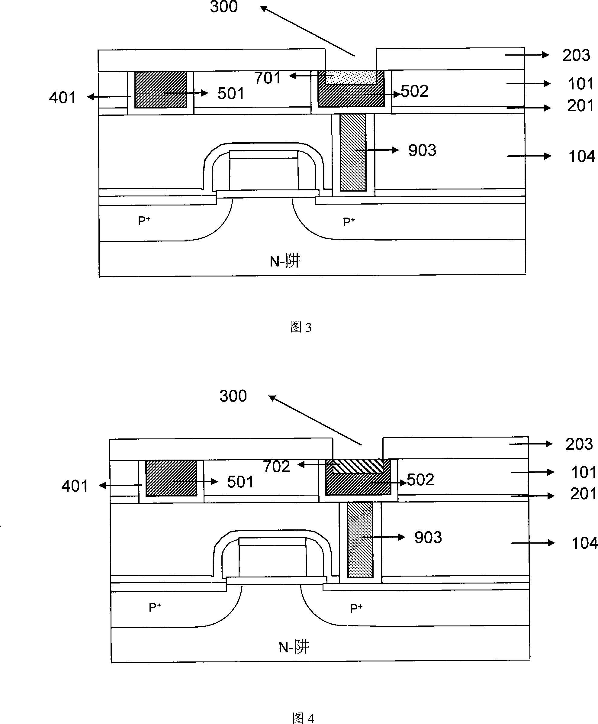
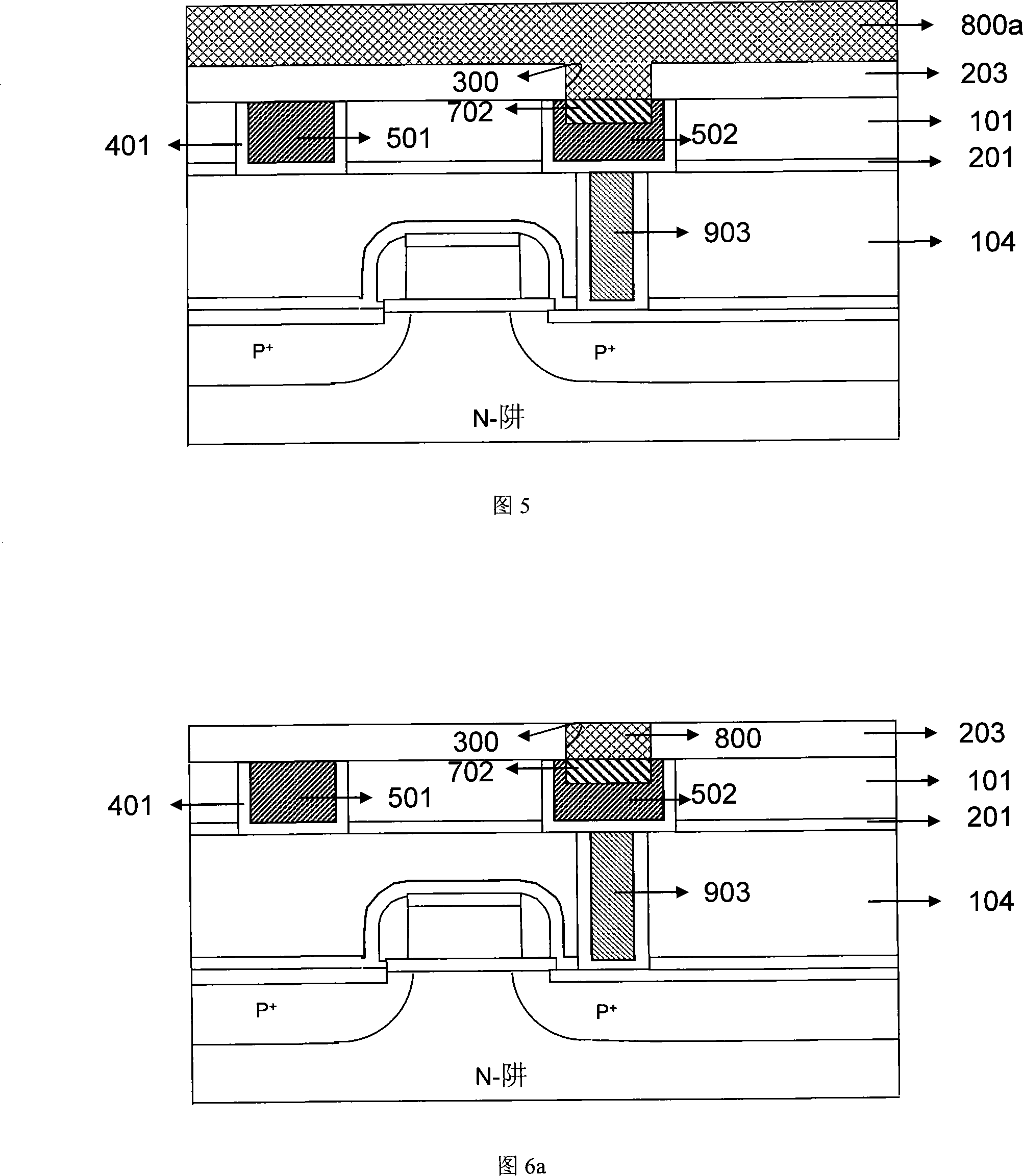
[0020] Hereinafter, the present invention will be more fully described in reference embodiments in conjunction with the drawings. The present invention provides preferred embodiments, but should not be considered as limited to the embodiments set forth herein. In the figure, the thickness of the layers and regions are enlarged for clarity, but as a schematic diagram, it should not be regarded as strictly reflecting the proportional relationship of geometric dimensions.

[0021] The reference figure here is a schematic diagram of an idealized embodiment of the present invention. The embodiment shown in the present invention should not be considered as limited to the specific shape of the area shown in the figure, but includes the resulting shape, such as caused by manufacturing. deviation. For example, the curve obtained by dry etching usually has the characteristics of bending or roundness, but in the illustrations of the embodiments of the present invention, they are all represe...


PUM


Abstract

The invention belongs to the field of microelectronic technology, in particular to a method for eliminating forming voltage of CuxO resistive memory. The method comprises following steps: growing CuxO memory medium, and annealing in oxygen-deficiency environment such as N2, Ar, forming gas or vacuum to reduce the surface CuO to Cu2O, thus eliminating forming voltage of the memory during the firstprogramming, reducing current and voltage of write operation, and preventing CuxO memory medium with resistance switch characteristics below the surface CuO layer from being damaged by high current. The method of the invention has the advantages of simple process, low cost and significantly improved fatigue characteristics of the CuxO resistive memory.

Description

Technical field [0001] The invention belongs to the technical field of microelectronics, and specifically relates to a method for eliminating Cu x The method of forming voltage for resistance memory. Background technique [0002] Memory occupies an important position in the semiconductor market. Due to the continuous popularization of portable electronic devices, the share of non-volatile memory in the overall memory market is also increasing, and more than 90% of the market is occupied by FLASH. However, due to the requirement of storing electric charges, the floating gate of FLASH cannot be thinned unlimitedly with the development of technology. According to reports, the limit of FLASH technology is predicted to be around 32nm, which forces people to search for next-generation non-volatile memories with superior performance. Recently, resistance switching memory devices (resistive switching memory) have attracted great attention because of their high density, low cost, and abil...

Claims


Application Information

Patent Timeline
Patent Type & Authority Patents(China)
IPC IPC(8): H01L45/00H01L27/24G11C11/56G11C16/02
Inventor 林殷茵陈邦明吕杭炳
Owner FUDAN UNIV
Why Eureka
Try Eureka