

Lens structure and light emitting unit
A lens structure and lens technology, applied in semiconductor devices, optics, light sources, etc. of light-emitting elements, to achieve improved light diffusion effects and good light diffusion effects
- Summary
- Abstract
- Description
- Claims
- Application Information
AI Technical Summary
Problems solved by technology
Method used
Image


Examples
Embodiment Construction
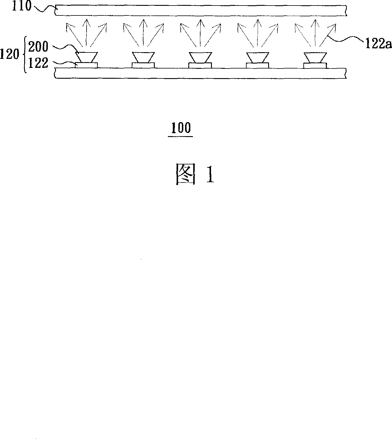
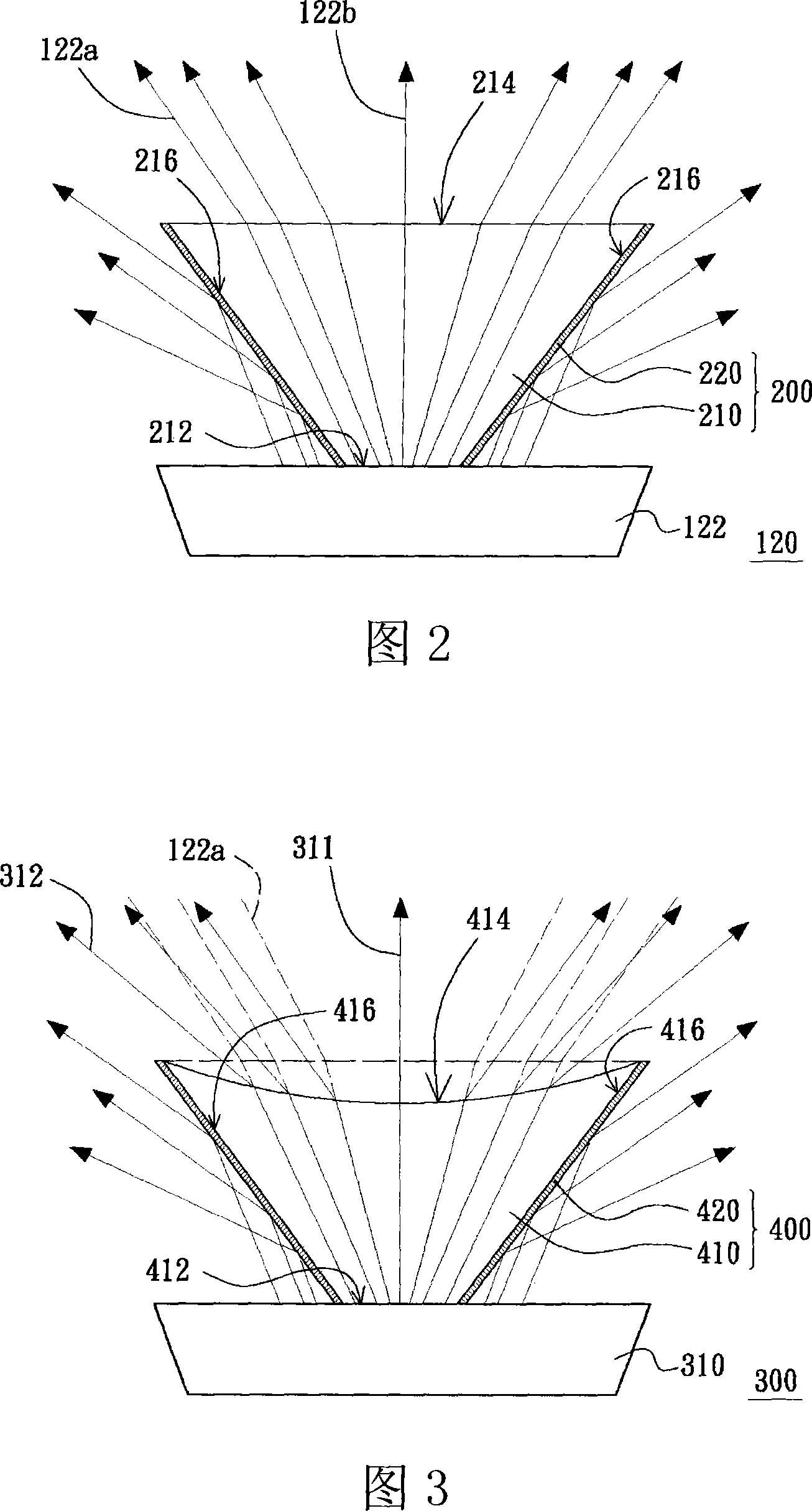
[0053] FIG. 3 is a schematic diagram of a light emitting unit according to an embodiment of the present invention. Referring to FIG. 3 , the light emitting unit 300 of this embodiment includes an LED light source module 310 and a lens structure 400 , wherein the lens structure 400 is disposed on the LED light source module 310 . The lens structure 400 includes a lens body 410 , and the lens body 410 has a light incident surface 412 , a light output surface 414 and a reflective surface 416 . The light incident surface 412 is opposite to the light exit surface 414 , and the reflective surface 416 is conical and connected between the light incident surface 412 and the light exit surface 414 . The area of the light incident surface 412 is smaller than that of the light exit surface 414 , and the light exit surface 414 is a concave curved surface.
[0054]In the aforementioned lens structure 400 , the light incident surface 412 is a plane, and the light incident surface 412 face...
PUM
| Property | Measurement | Unit |
|---|---|---|
| Radius of curvature | aaaaa | aaaaa |
| Particle size | aaaaa | aaaaa |
Abstract
Description
Claims
Application Information