Optical film and manufacturing method thereof

A manufacturing method and technology of optical film, applied in optics, optical components, nonlinear optics, etc., can solve problems such as unfavorable production, inability to combine optical film layers firmly, and difficult process, so as to shorten the curing time of the film layer, improve the Light diffusion effect, effect of increasing surface roughness

Active Publication Date: 2010-09-15
ZHEJIANG JINHUI OPTOELECTRONIC MATERIAL CO LTD
View PDF17 Cites 11 Cited by
  • Summary
  • Abstract
  • Description
  • Claims
  • Application Information

AI Technical Summary

Problems solved by technology

[0005] Since forming each film layer must go through the film curing process, the process time of the above-mentioned optical film is long and the efficiency is slow, resulting in the lack of production capacity and high manufacturing cost.
Moreover, the light-collecting layer and the base material are made of different materials, and the base material and the diffusion layer are also made of different materials. The combination of layers of different materials must also consider the stability of the combination, so the number of layers of the optical film increases. It will be more difficult to manufacture for a long time, so its manufacturing process is more difficult. If there is any defect in the manufacturing process, it may cause the various layers of the optical film to be unable to be firmly combined

Method used


Image

  • Optical film and manufacturing method thereof
  • Optical film and manufacturing method thereof
  • Optical film and manufacturing method thereof

Examples


Embodiment Construction

[0024] The present invention will be described in detail below with reference to the accompanying drawings and embodiments. It should be noted that in the following description, similar elements are denoted by the same numerals.

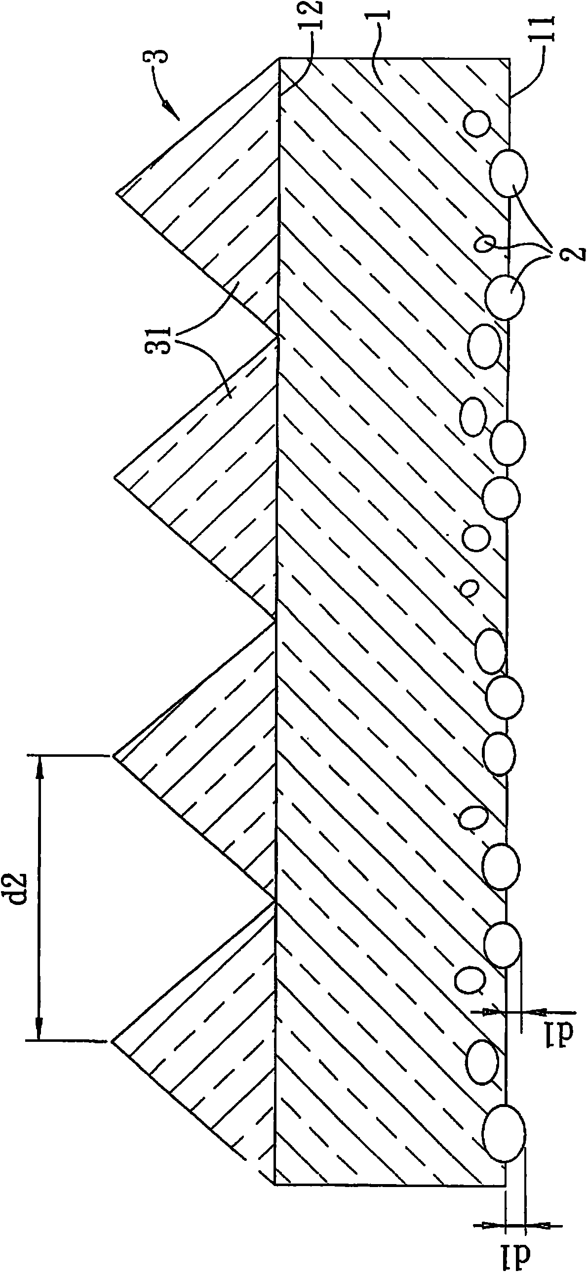
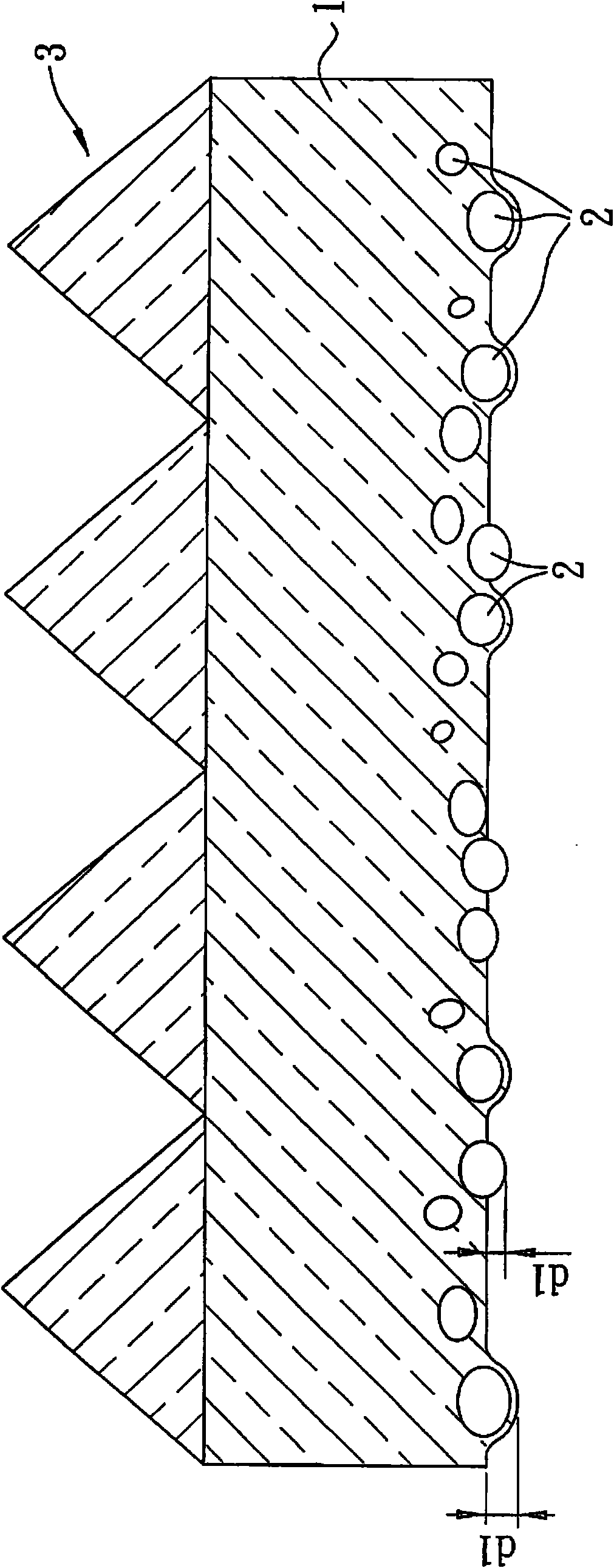
[0025] refer to figure 1 , The first preferred embodiment of the optical film of the present invention includes: a substrate 1 , a plurality of diffusion particles 2 distributed on the substrate 1 , and a light-collecting layer 3 disposed on the surface of the substrate 1 .

[0026] The substrate 1 includes a first surface 11 and a second surface 12 spaced in opposite directions. The first surface 11 faces a light source not shown in the figure, and the light emitted by the light source passes through the substrate 1 and the set in sequence. The optical layer 3, but the embodiment is not limited by the relative position of the light source and the optical film of the present invention. Although the second surface 12 of the base material 1 in this em...


PUM

PropertyMeasurementUnit
particle diameteraaaaaaaaaa
thicknessaaaaaaaaaa

Abstract

The invention relates to an optical film and a manufacturing method thereof, which comprises a light-permeable base material, a plurality of diffusion micro-particles distributed on the base material and a light collection layer arranged on the surface of the base material. Part of the diffusion micro-particles lead at least one surface of the base material to form bulges, and the protrusive height of part of the bulges is larger than or equal to 0.5 mu m. The manufacturing method of the optical film mainly comprises the following steps: heating the base material for leading the base material to be in molten state, adding the diffusion micro-particles on the surface of the base material, curing the base material for forming the base material, and finally forming the light collection layer on the surface of the base material. The optical film only contains the double-layer structure of the base material and the light collection layer, and can still achieve the effects of light collection and light diffusion atomization while reducing the number of film layers, so that the manufacturing method has the advantages of easy manufacture and reduced cost.

Description

technical field [0001] The invention relates to an optical film and a manufacturing method thereof, in particular to an optical film which is applied to a display and has both light collection and light diffusion and atomization functions and a manufacturing method thereof. Background technique [0002] Both the brightness enhancement film and the diffusion film are important components in a liquid crystal display (LCD). The brightness enhancement film is used to make the light emitted in a relatively concentrated manner, and concentrated in the range of the user's viewing angle, so as to increase the brightness of the LCD. On the other hand, since there are multiple layers of optical films stacked in the module, the optical interference between the films is likely to produce Newton-rings (Newton-ring), or the film itself will have optical defects such as rainbow lines, so it must be passed The light diffusion and atomization effect of the diffusion film prevents the above-m...

Claims


Application Information

Patent Timeline
Patent Type & Authority Applications(China)
IPC IPC(8): G02B6/00G02B5/02F21V5/02G02F1/13357
Inventor 伍清钦吴宗勋郑闵玮
Owner ZHEJIANG JINHUI OPTOELECTRONIC MATERIAL CO LTD
Why Eureka
Try Eureka