Semiconductor testing device, performance board and interface plate

A test device and semiconductor technology, applied in the field of interface boards, can solve problems such as large use

Inactive Publication Date: 2008-08-06
ADVANTEST CORP
View PDF1 Cites 2 Cited by
  • Summary
  • Abstract
  • Description
  • Claims
  • Application Information

AI Technical Summary

Problems solved by technology

In addition, there is a problem that a large force is sometimes required to connect the connectors at the same time.

Method used


Image

  • Semiconductor testing device, performance board and interface plate
  • Semiconductor testing device, performance board and interface plate
  • Semiconductor testing device, performance board and interface plate

Examples


Embodiment Construction

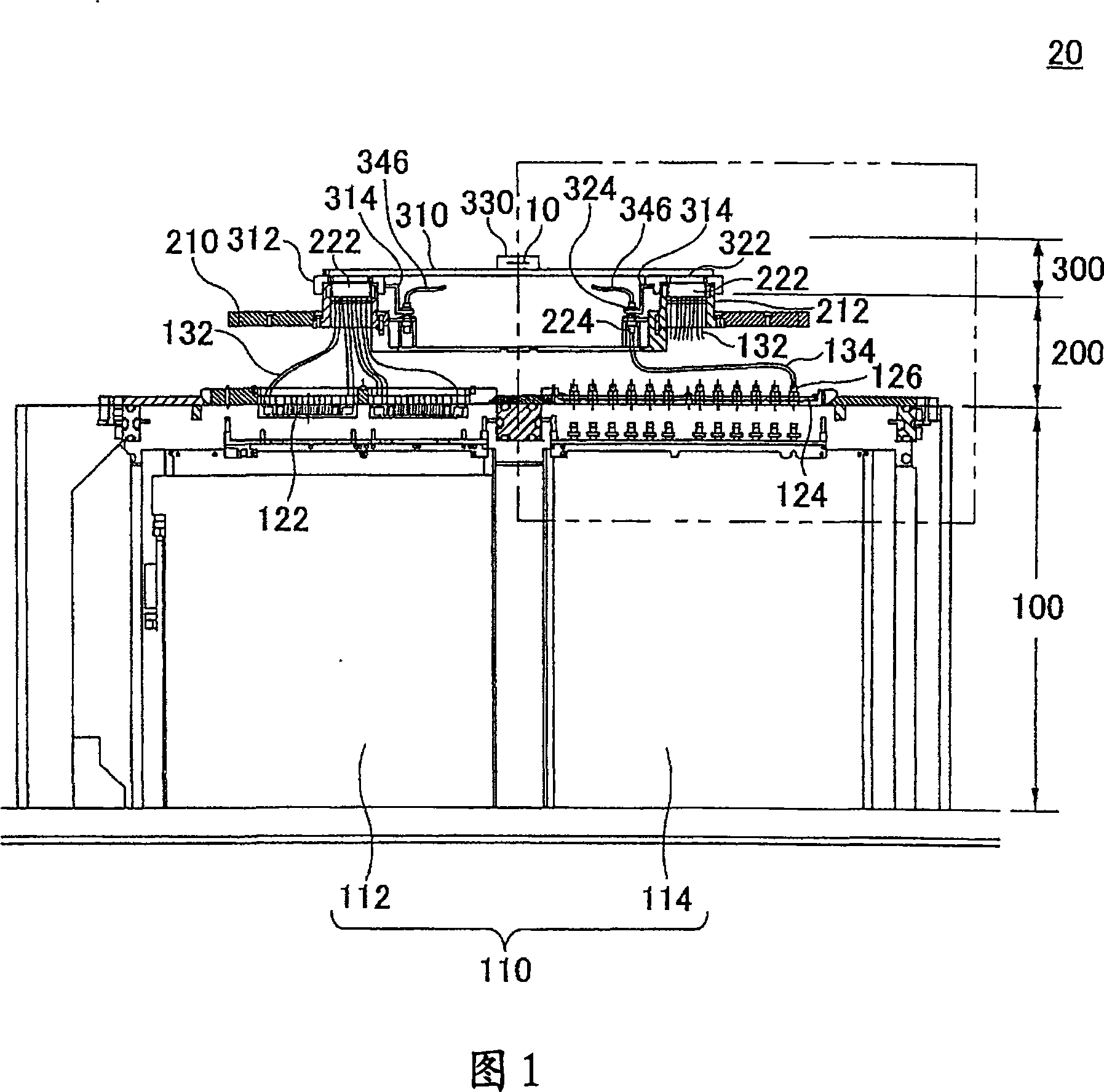
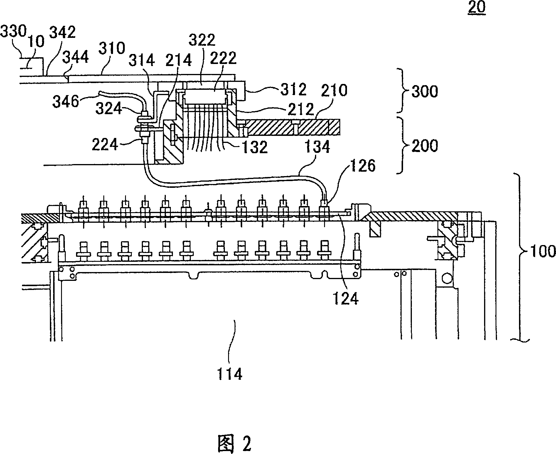
[0072] Hereinafter, the present invention will be explained through the embodiments of the invention. However, the following embodiments are not intended to limit the scope of the claims, and combinations of the features of the invention in the embodiments are not all necessary solutions for the invention.

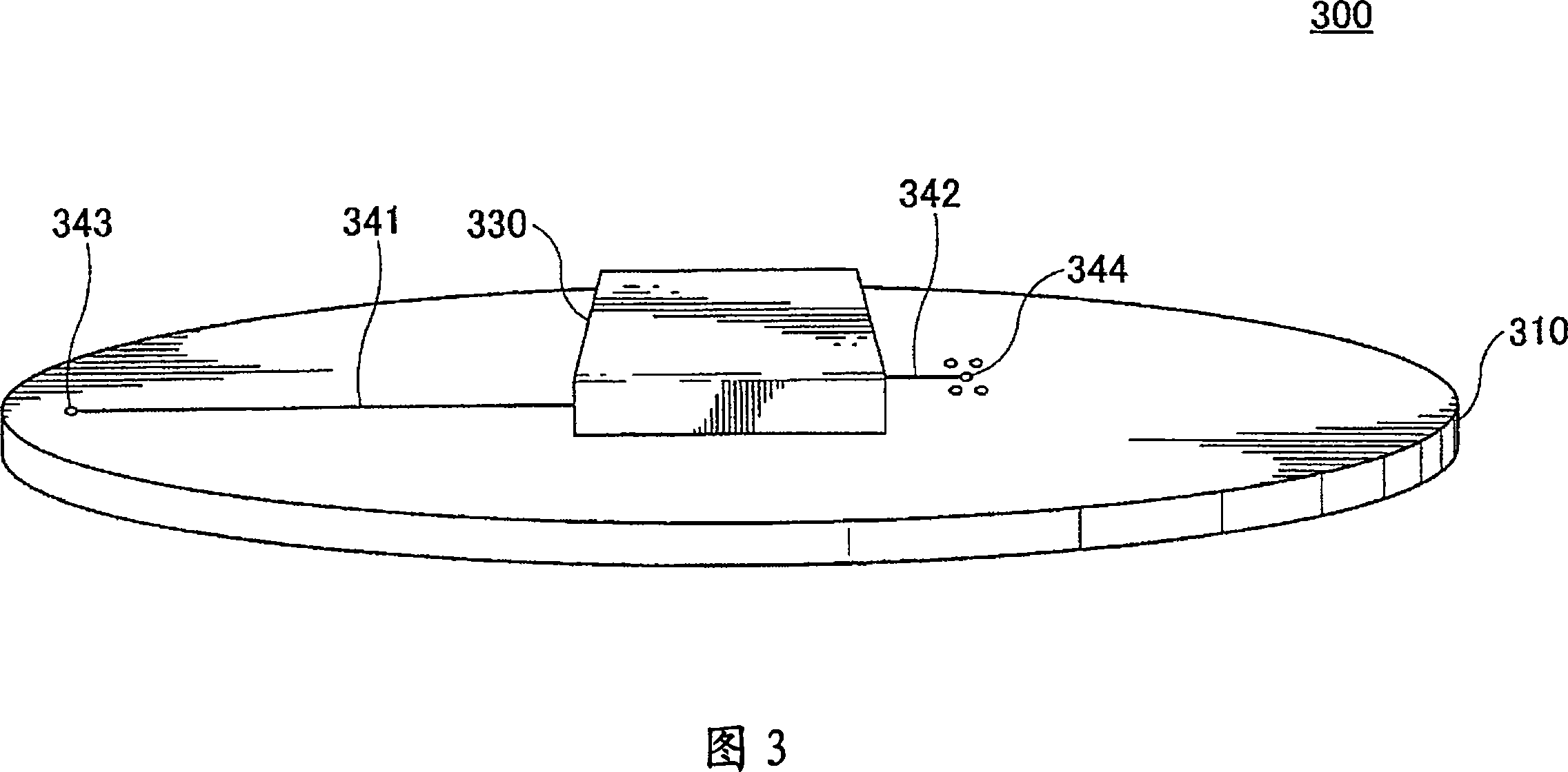
[0073] FIG. 1 is a schematic partial cross-sectional view of a semiconductor testing device 20 according to the present embodiment. As shown in the figure, the semiconductor test device 20 is stacked sequentially on the test head body 100 to form an interface board 200 and a function board 300 .

[0074] However, this embodiment revolves around the case where test signals of different frequencies or powers are used for the connection terminals of one device under test 10, that is, for example, when a common analog or digital test signal (A / D (analog and digital) is used. ) test signal) while performing a test using the RF (Radio Frequency) band. In this case, the electric...


PUM


Abstract

The invention provides a semiconductor testing device (20) capable of connecting different types of connectors of a function board (200) at one time. Described device has: test head body (100), and described test head body (100) comprises the signal assembly (110) that sends the test signal that is used for testing device under test (10); Interface board (200), and it has and The board body (210) and the signal component (110) are electrically connected, and are arranged on a plurality of sockets on the board body (210), and are installed on the test head body (100); and, the function board (300), the The functional board (300) has a connector on one side that is embedded and electrically connected to the socket, and the other side has a test socket (330) that is electrically connected to the connector and connected to the device under test (10). The device is fitted on the socket and installed on the interface board (200); the device also includes a lifting socket and a lifting connector that are displaced relative to the board body (200) in the direction of plugging and unplugging the connector to the socket.

Description

technical field [0001] The present invention relates to a semiconductor device and an interface plate. In more detail, it relates to a semiconductor test device for performing a test of a device to be tested by inputting and outputting a test signal between devices to be tested, and an interface board mountable on such a semiconductor test device. For the designated countries that recognize the addition of content through document reference, the content described in the following applications is incorporated by reference as a part of this application. [0002] 1. Special petition: 2005-228289, application date: August 5, 2005 Background technique [0003] Generally, semiconductor devices are subjected to test quality control during the manufacturing process and before shipment. In such a test, the device under test is temporarily mounted on a semiconductor test device, and the test is performed by inputting and outputting a test signal between a signal module provided on t...

Claims


Application Information

Patent Timeline
Patent Type & Authority Applications(China)
IPC IPC(8): G01R31/28
CPCG01R31/2889G01R31/26H01L22/00
Inventor 伊藤良真林省三
Owner ADVANTEST CORP
Why Eureka
Try Eureka