Supercharge Your Innovation With Domain-Expert AI Agents!

Shift buffer

A technology of a shift register and a shift register unit, which is used in instruments, static indicators, and logic circuit coupling/interface using field effect transistors, etc., can solve the problem of incorrect output signals and the inability of the shift register unit 1 to operate normally. And other issues

Active Publication Date: 2008-08-27
AU OPTRONICS CORP
View PDF0 Cites 10 Cited by
  • Summary
  • Abstract
  • Description
  • Claims
  • Application Information

AI Technical Summary

Problems solved by technology

When the threshold voltage of the transistor of the shift register unit 1 deviates, the shift register unit 1 cannot operate normally, resulting in an incorrect output signal S N

Method used


Image

  • Shift buffer
  • Shift buffer
  • Shift buffer

Examples


Embodiment Construction

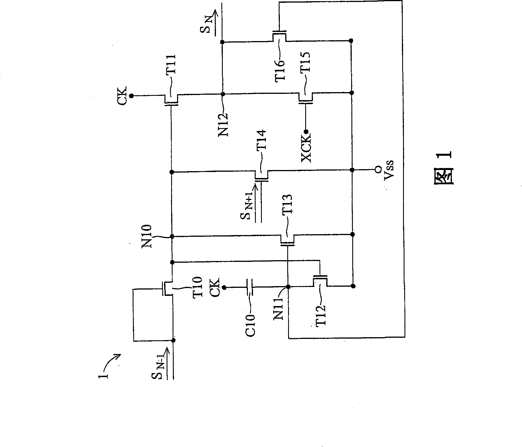
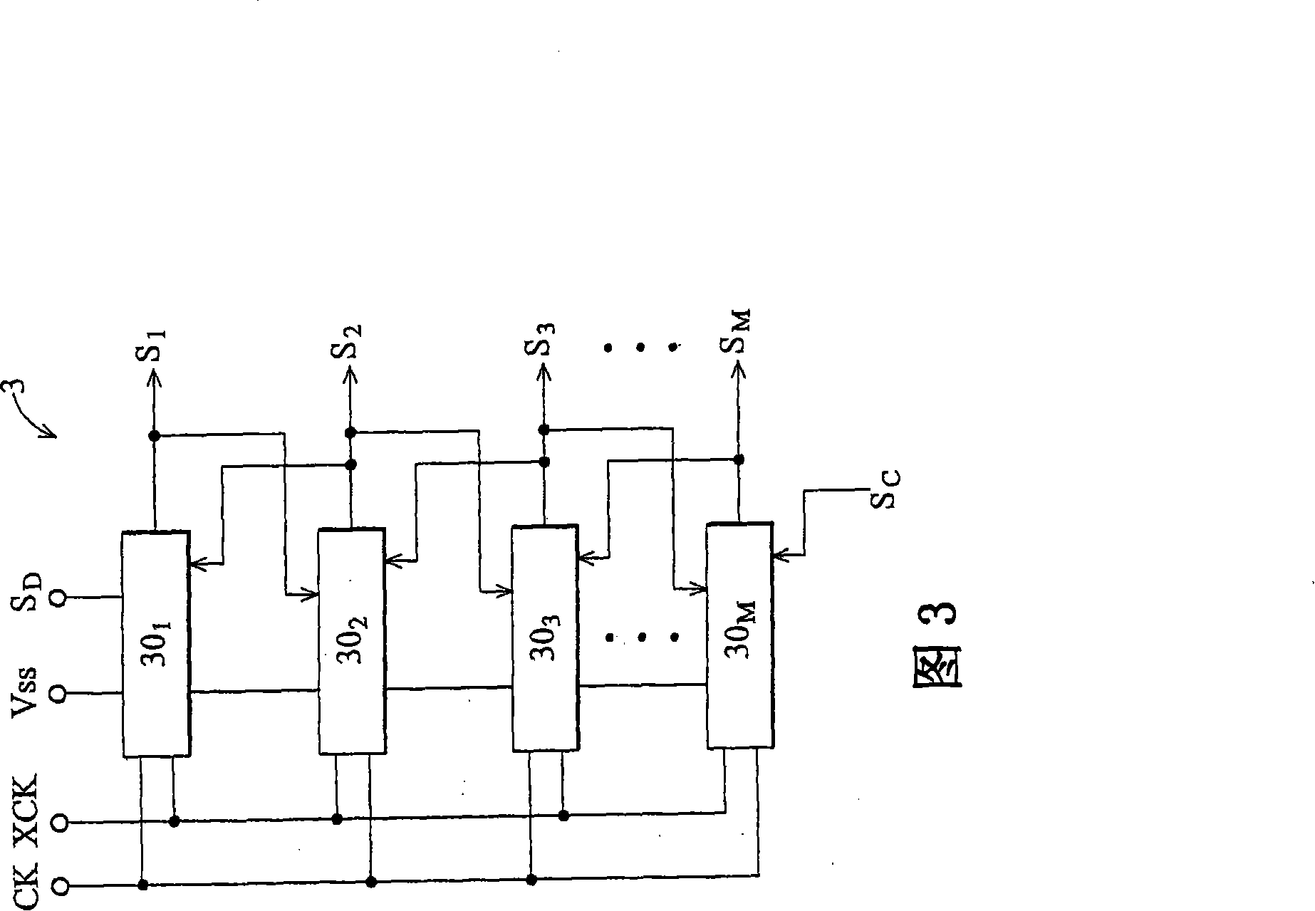
[0025] FIG. 3 shows a shift register according to the present invention, which is suitable for a liquid crystal display panel. Referring to Fig. 3, the shift register 3 includes a plurality of serially connected shift register units 30 1 -30 M . Each shift register unit is controlled by clock signals CK and XCK, and is coupled to a voltage source Vss. Each shift register unit receives a first input signal and a second input signal, and generates an output signal according to mutually inverse clock signals CK and XCK. Shift buffer unit 30 1 -31 M The resulting output signal S 1 -S M are activated sequentially, and each output signal is activated periodically.

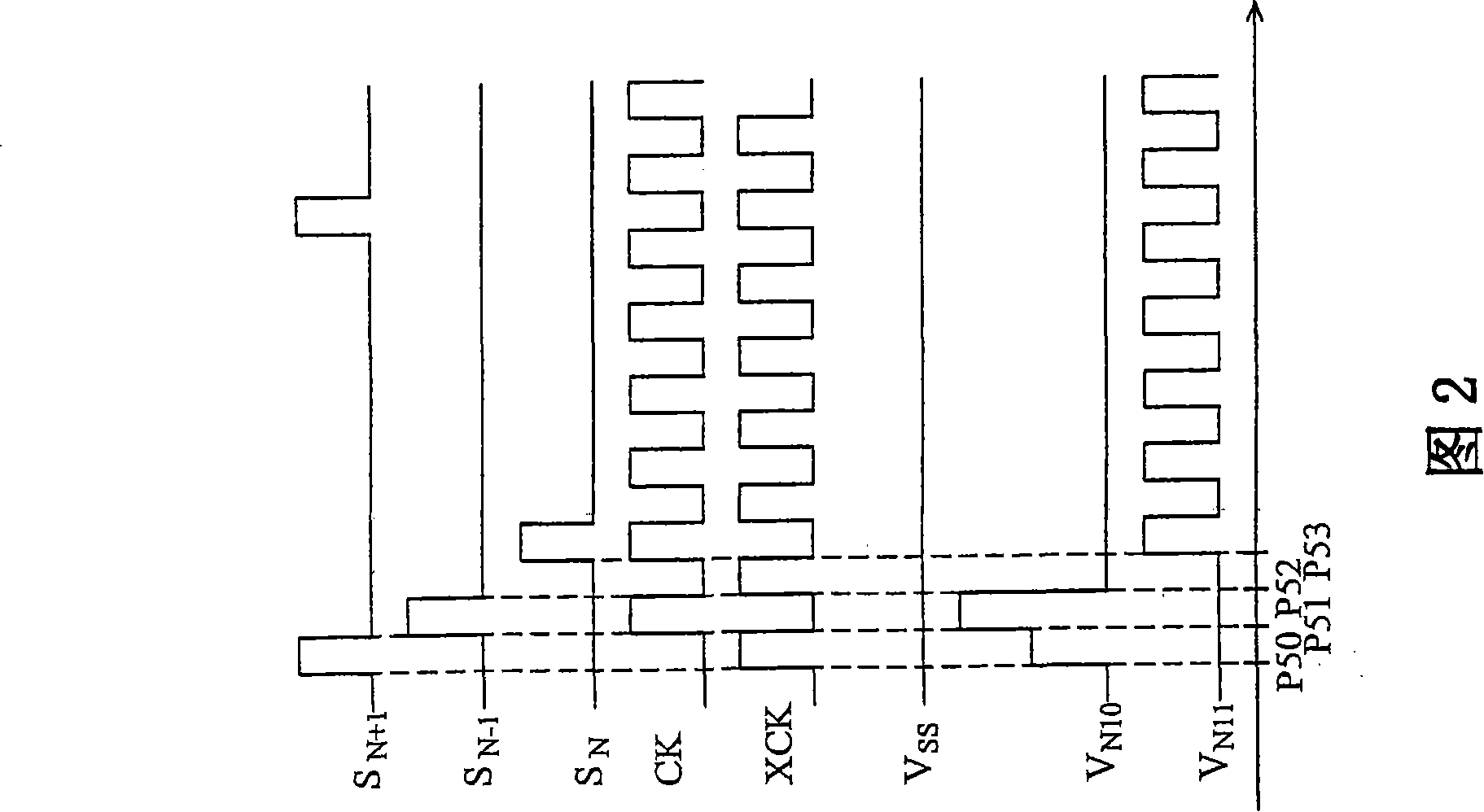
[0026] Shift buffer unit 30 2 -30 M 30 each N (1N-1 The resulting output signal S N-1 Take it as the first input signal, and receive the shift register unit 30 of the next stage N+1 The resulting output signal S N+1 Take as the second input signal, where the output signal S N-1 , S N , S N+1 are activated...


PUM


Abstract

Disclosed is a shift buffer, comprising shift buffering units which are sequentially connected in series. Each shift buffering unit, composed of a first and a second switch gears and a first and a second driving devices, generates output signals under the control of a first and a second time-pulse signals which are opposite to each other. The first switchgear provides output signals through an output node. The first driving device drives the first switchgear to activate the output signals according to the first input signal; the second driving device is coupled with a first voltage signal and conveys the first voltage signal according to the first time pulse signal to drive the first switchgear to not activate the output signals. When the first switchgear does not activate the output signals, the second switchgear provides a second voltage signal to the output node according to the second time-pulse signal. The level of the first voltage signal is lower than the level of the second voltage signal. The shift buffer can avoid the occasion that the shift buffering units are out of normal work when the critical voltage of the transistor offset.

Description

technical field [0001] The present invention relates to a shift register, in particular to a shift register unit, the output signal of which is not affected by the shift of the critical voltage of the internal transistor. Background technique [0002] In the current LCD panel design, the scan signal and the data signal are generated by the gate driver and the source driver. In order to reduce the cost, a shift register with the same circuit function as the gate driver is arranged on the glass substrate. However, since the shift register mostly adopts the technology of amorphous silicon thin film process, after the display panel is lit, the panel display is abnormal due to the influence of stress on the transistor. [0003] Fig. 1 shows a shift register unit of a known shift register. FIG. 2 is a signal timing diagram showing a known shift register unit. Referring to FIG. 1 and FIG. 2 , the shift register unit 1 is controlled by clock signals CK and XCK which are opposite ...

Claims


Application Information

Patent Timeline
IPC IPC(8): H03K19/0175H03K19/0185H03K19/003G09G3/36
Inventor 郑国兴胡维宾李国贤李纯怀
Owner AU OPTRONICS CORP
Features
  • R&D
  • Intellectual Property
  • Life Sciences
  • Materials
  • Tech Scout
  • Unparalleled Data Quality
  • Higher Quality Content
  • 60% Fewer Hallucinations
Learn More