Cell test method and liquid crystal display panel for a tri-gate type pixel structure

一种液晶显示面板、测试方法的技术,应用在机器/结构部件的测试、光学仪器测试、测量装置等方向,能够解决无法依序分别点亮红/绿/蓝子画素、短路杆波形编辑顺序无法应用薄膜晶体管液晶显示器等问题

Active Publication Date: 2013-04-10
HANNSTAR DISPLAY CORPORATION
View PDF4 Cites 18 Cited by
  • Summary
  • Abstract
  • Description
  • Claims
  • Application Information

AI Technical Summary

Problems solved by technology

However, the above-mentioned panel testing method and the waveform editing sequence of the short-circuit bar cannot be applied to a thin-film transistor liquid crystal display with a tri-gate pixel structure because the red data line D is used in a single-gate pixel structure. R , green data line D G and blue data line D B Control the red / green / blue sub-pixels R / G / B, but the three-gate pixel structure is changed to use the red gate line G R , green gate line G G and blue gate line G B Drive red / green / blue sub-pixel R / G / B
If the shorting bar test is also used for the three-gate pixel structure panel test, the shorting bar waveform editing sequence for the single-gate pixel structure cannot be used to light up the red / green / blue sub-pixels R / G / B

Method used


Image

  • Cell test method and liquid crystal display panel for a tri-gate type pixel structure
  • Cell test method and liquid crystal display panel for a tri-gate type pixel structure
  • Cell test method and liquid crystal display panel for a tri-gate type pixel structure

Examples


Embodiment Construction

[0070] In order to make the above-mentioned features and advantages of the present invention more comprehensible, the following specific embodiments are described in detail with reference to the accompanying drawings.

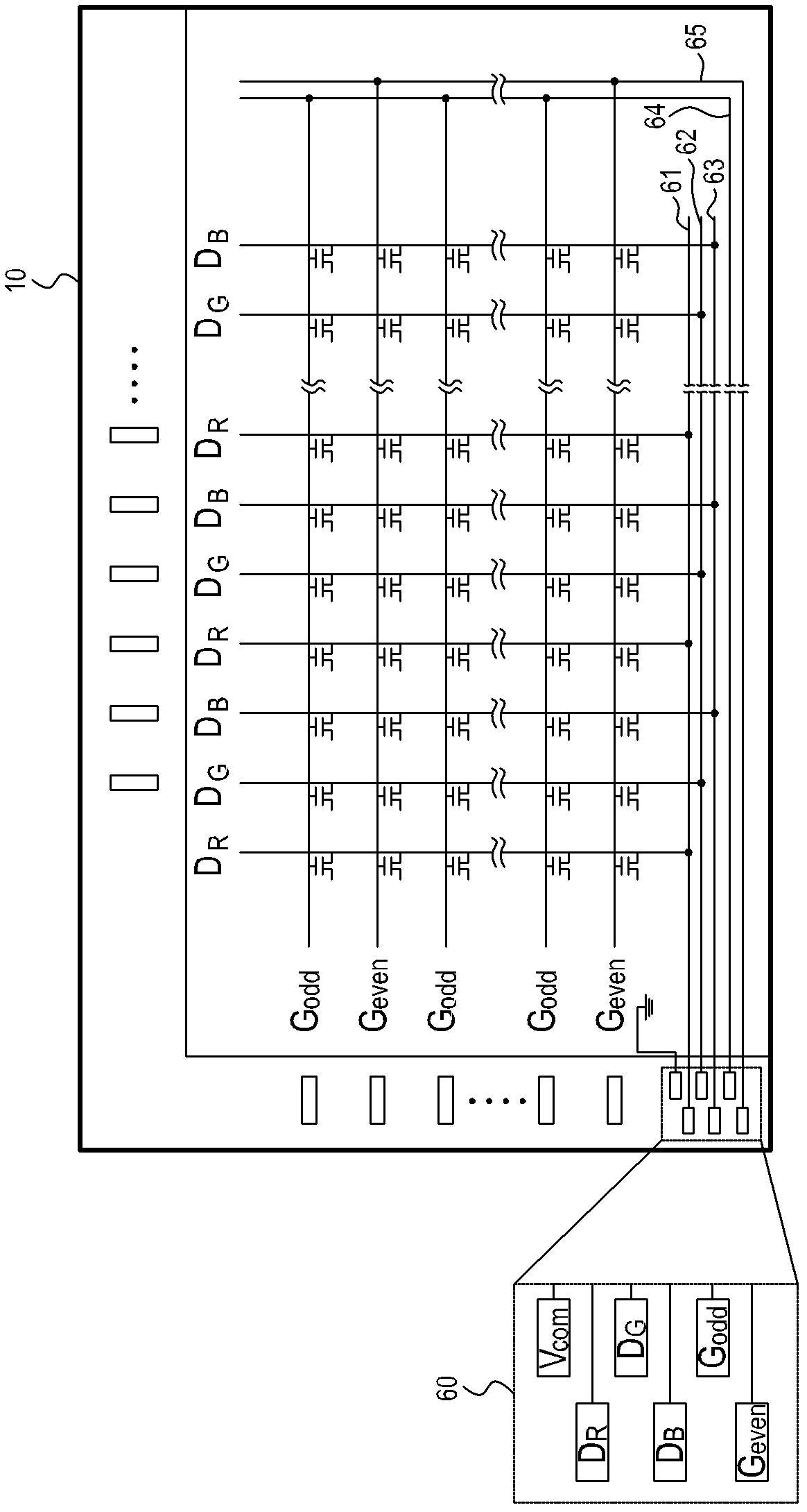
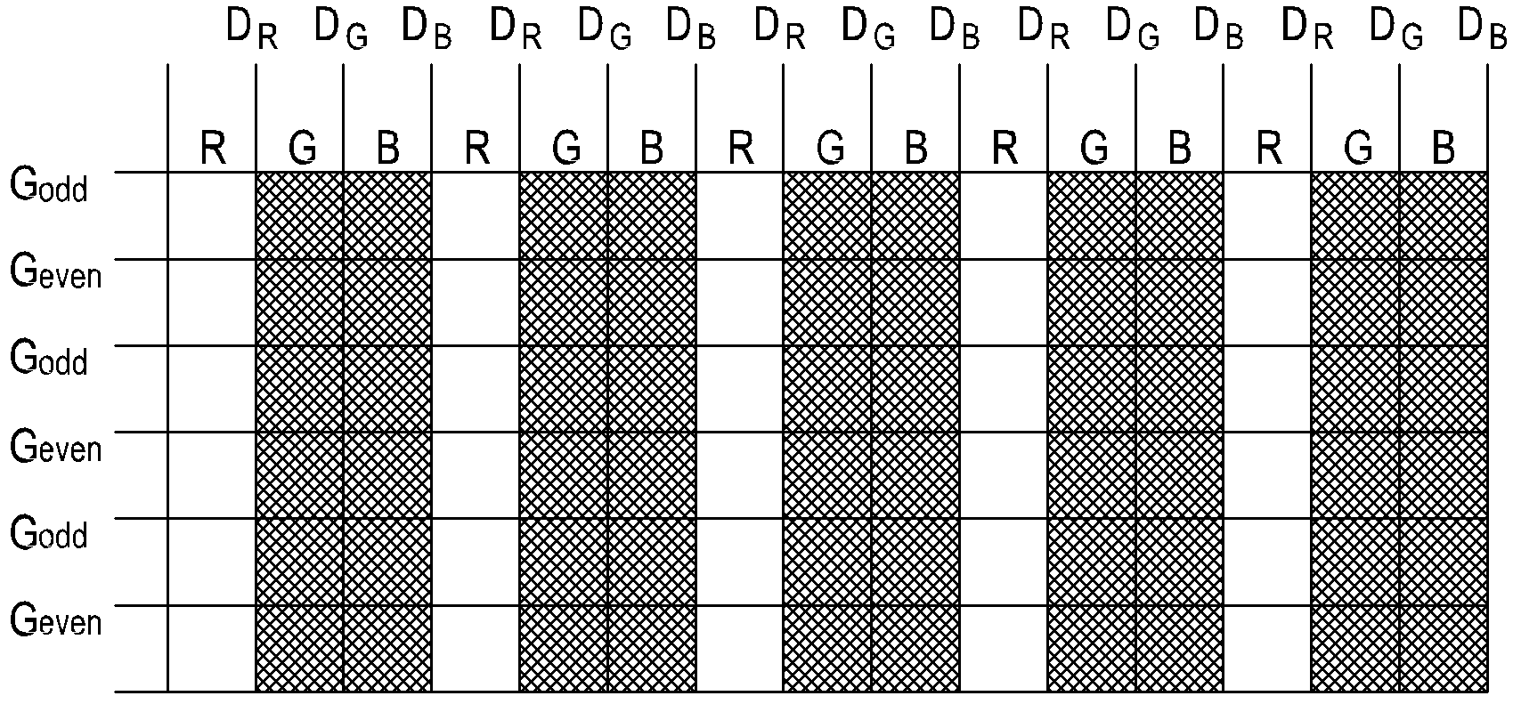
[0071] Please refer to Figure 9 , which shows a schematic plan view of a liquid crystal display panel 110 with a three-gate pixel structure according to an embodiment of the present invention. Taking the resolution n*m as an example, the liquid crystal display panel 110 with a three-gate pixel structure has m*3 gate lines (scanning lines) G 1 , G 2 , G 3 , G 4 …G 3m-2 , G 3m-1 , G 3m , and n data lines D 1 、D 2 、D 3 、D 4 …D n-2 、D n-1 、D n . Such as figure 1 As shown, gate line G 1 , G 2 , G 3 , G 4 …G 3m-2 , G 3m-1 , G 3m with data line D 1 、D 2 、D 3 、D 4 …D n-2 、D n-1 、D n Define 3*m*n sub-pixels. The sub-pixels are red sub-pixel R, green sub-pixel G and blue sub-pixel B. Gate line G 1 , G 2 , G 3 , G 4 …G 3m-2 , G 3m-1 ...


PUM


Abstract

A cell test method for a liquid crystal display panel includes the following steps. A waveform sequence to shorting bars is provided, wherein the waveform sequence includes that the first gate line sends a voltage of turn on signal and the second and third gate lines send a voltage of turn off signal at the first and second time periods; and the waveform sequence further comprises that the first and second data lines respectively send first and second voltages at the first and second time periods, the first threshold voltage is higher than the first voltage, the first voltage is higher than the common voltage, the common voltage is higher than the second voltage, and the second voltage is higher than the second threshold voltage, whereby pixels defined by the first gate line and the first and second data lines is turn on.

Description

technical field [0001] The invention relates to a panel testing method for a liquid crystal display with a three-gate pixel structure, in particular to a testing method for a liquid crystal display panel with a three-gate pixel structure and the liquid crystal display panel. Background technique [0002] The manufacture of liquid crystal display panels includes array (array) process, panel (cell) process and module (module) process. After each process is completed, testing will be carried out to eliminate unqualified products. [0003] Please refer to figure 1 , which shows a schematic plan view of a liquid crystal display panel 10 in the prior art. The test pad 60 for panel detection is disposed in the non-display area of ​​the liquid crystal display panel 10 . When the panel detection uses the shorting bar (shorting bar) detection, the odd number of gate lines G odd and an even number of gate lines G even (that is, the scan line) signal is separated, and the red data l...

Claims


Application Information

Patent Timeline
Patent Type & Authority Applications(China)
IPC IPC(8): G02F1/13G01M11/00
CPCG09G3/36G09G2300/0426G09G3/006
Inventor 吕泰福
Owner HANNSTAR DISPLAY CORPORATION
Why Eureka
Try Eureka