Unlock instant, AI-driven research and patent intelligence for your innovation.

Electronic part encapsulation module, external cover and its making method

A technology for electronic components and packaging modules, which is applied in the field of outer covers of electronic component packaging modules, and can solve problems such as unavoidable

Active Publication Date: 2008-09-10
ADVANCED SEMICON ENG INC
View PDF1 Cites 1 Cited by
  • Summary
  • Abstract
  • Description
  • Claims
  • Application Information

AI Technical Summary

Problems solved by technology

In addition, the dielectric material layer 145 of the ground arc 170 does not cover the entire component area 112 of the substrate, so the dielectric material layer 145 can only prevent the conductive material layer 160 from contacting the bonding wires 120, but cannot prevent The conductive material layer 160 contacts other components located on the component region 112 of the substrate 110

Method used


Image

  • Electronic part encapsulation module, external cover and its making method
  • Electronic part encapsulation module, external cover and its making method
  • Electronic part encapsulation module, external cover and its making method

Examples


Embodiment Construction

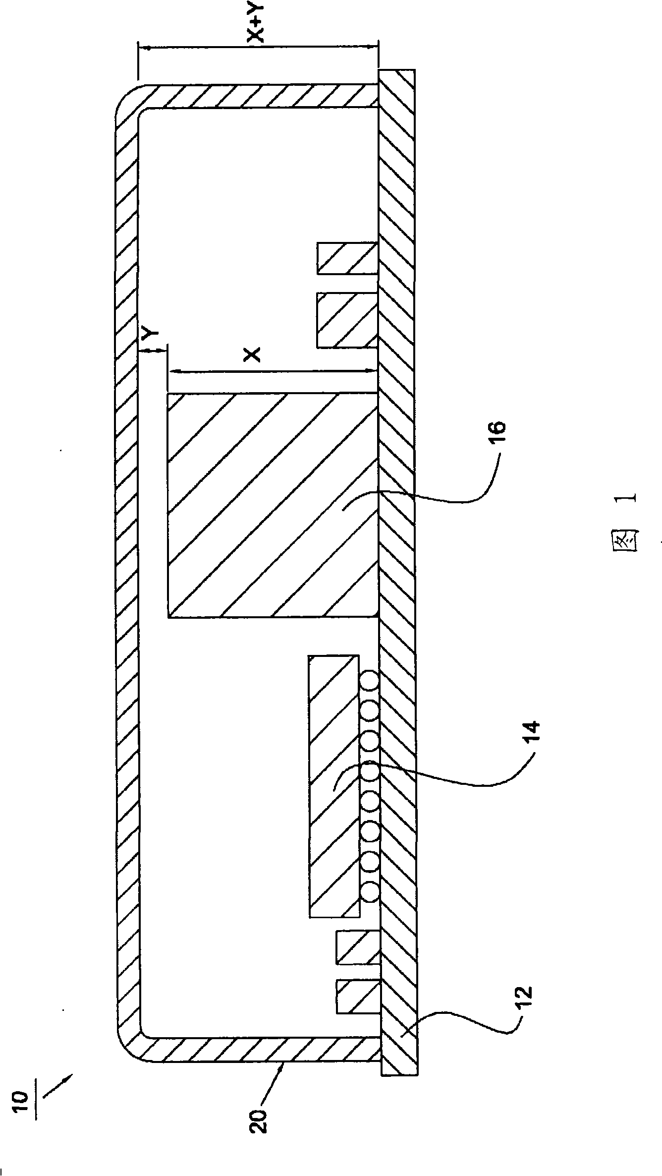
[0037] refer to image 3 , which shows an outer cover 220 according to an embodiment of the present invention. The outer cover 220 includes an inner layer 222 and an outer layer 224 . The outer layer 224 is disposed on the surface 223 of the inner layer 222 to form an outer cover 220 . The outer cover 220 has a top 226 and an annular supporting portion 228 , and the annular supporting portion 228 is connected to the top 226 .

[0038] The inner layer 222 and the outer layer 224 are respectively made of a non-conductive material and a conductive material. The conductive material may be a metal, such as copper or iron metal. The non-conductive material is non-metal, such as plastic or rubber.

[0039] The manufacturing method of the outer cover 220' of an embodiment of the present invention comprises the following steps: first, refer to Figure 4 , providing an inner layer 222 as a base layer. refer to Figure 5 , an outer layer 224 is formed on the surface 223 of the inn...


PUM


Abstract

The invention discloses an electronic element encapsulating module, an outer cover and a manufacturing method of the outer cover. The electronic element encapsulating module comprises a loader, at least one electronic element and the outer cover. The loader is provided with a first area and a second area. The electronic element is arranged at the first area of the loader. The outer cover is fixed at the second area of the loader and comprises an inner layer and an outer layer, wherein, the inner layer of the outer cover is made from non-conducting material and an outer layer thereof is made from conducting material; furthermore, the inner layer made from the non-conducting material covers the electronic element and the whole first area of the loader. According to the outer cover of the invention, the inner layer made from the non-conducting material can prevent the outer layer made from the conducting material from contacting all elements on the first area (also called element area) of the loader. When the electronic element encapsulating module is tested, the outer layer made from the conducting material does not contact a passive element and not cause short pass due to the application of pressure and external force.

Description

technical field [0001] The present invention relates to an electronic component packaging module, more particularly to an outer cover of an electronic component packaging module, the inner layer made of non-conductive material can prevent the outer layer made of conductive material from contacting the component area of ​​the carrier All components are used to avoid short circuit, and the outer layer made of conductive material can achieve the effect of metal shielding. Background technique [0002] Referring to FIG. 1 , it shows a wireless communication package module 10 . The wireless communication packaging module 10 includes a substrate 12 , a plurality of active components 14 and passive components 16 and an outer cover 20 . The active components 14 and the passive components 16 are assembled on the substrate 12 through a surface mount technology (SMT) process or an electronic packaging process. The outer cover 20 is fixed on the substrate 12 to cover the active compon...

Claims


Application Information

Patent Timeline
Patent Type & Authority Applications(China)
IPC IPC(8): H01L25/00H01L25/16H01L23/552H01L23/06H01L23/02H01L23/04H01L21/48
CPCH01L23/552H01L2224/16225H01L2924/19105
Inventor 陈建成
Owner ADVANCED SEMICON ENG INC
Features
  • R&D
  • Intellectual Property
  • Life Sciences
  • Materials
  • Tech Scout
  • Unparalleled Data Quality
  • Higher Quality Content
  • 60% Fewer Hallucinations
Learn More