Protruding block structure on base board
A technology of bumps and substrates, which is applied in the direction of electrical components, electrical solid devices, circuits, etc., and can solve problems such as the inability to detect the size of the gap between the glass and the wafer
- Summary
- Abstract
- Description
- Claims
- Application Information
AI Technical Summary
Problems solved by technology
Method used
Image

Examples
no. 1 example
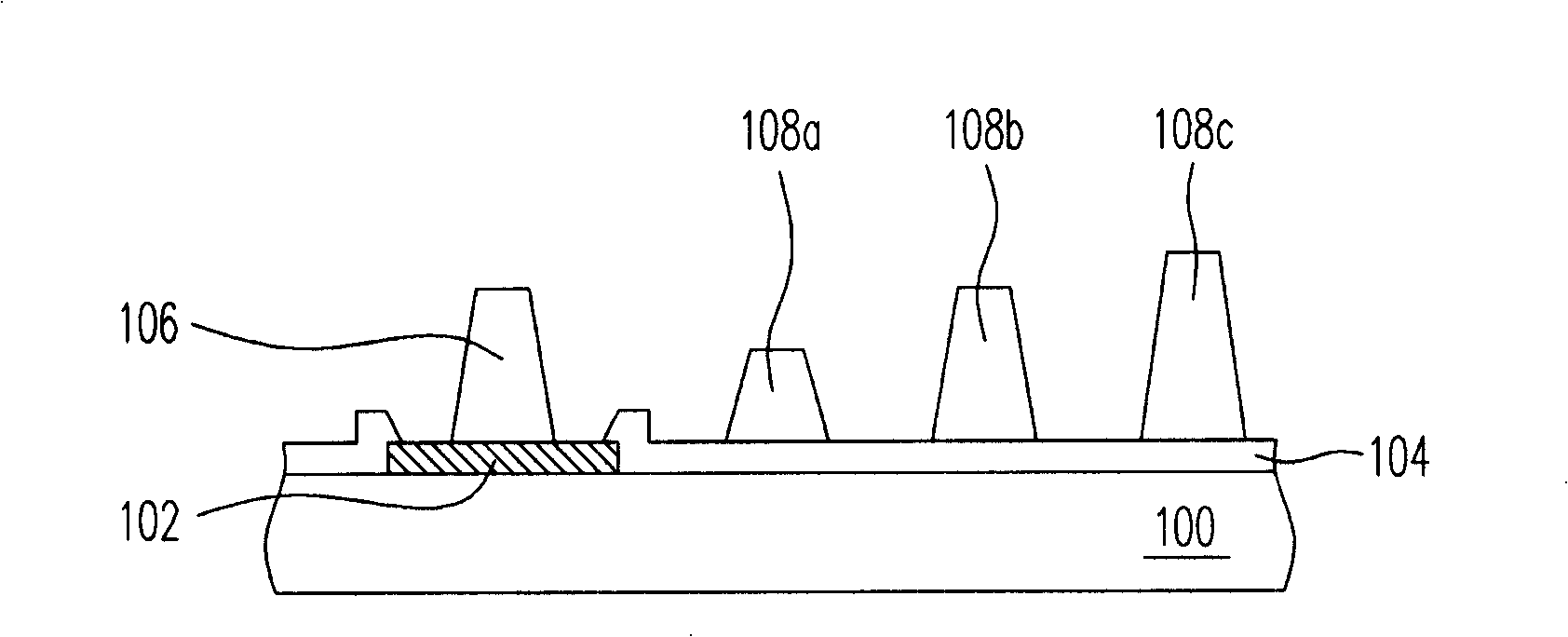
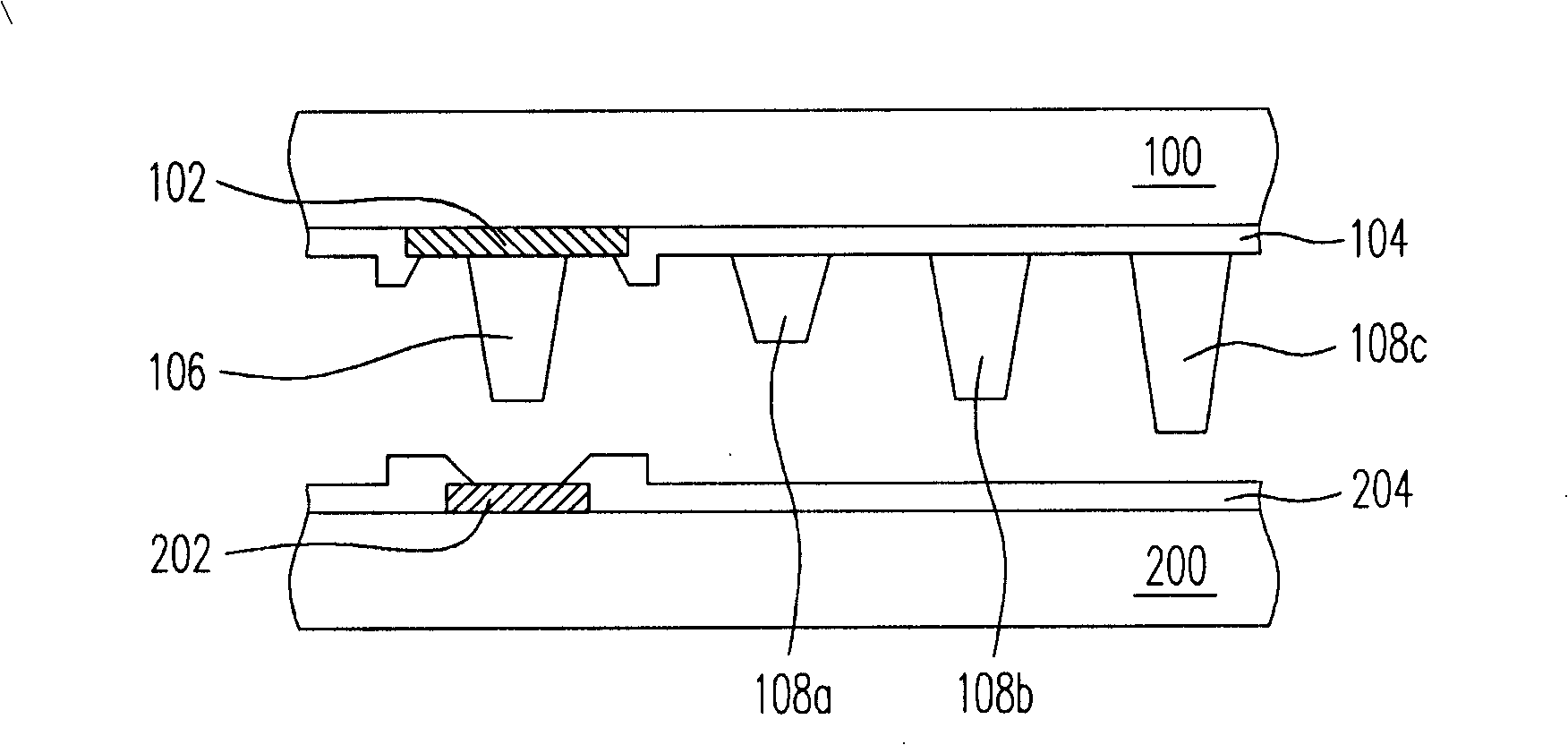
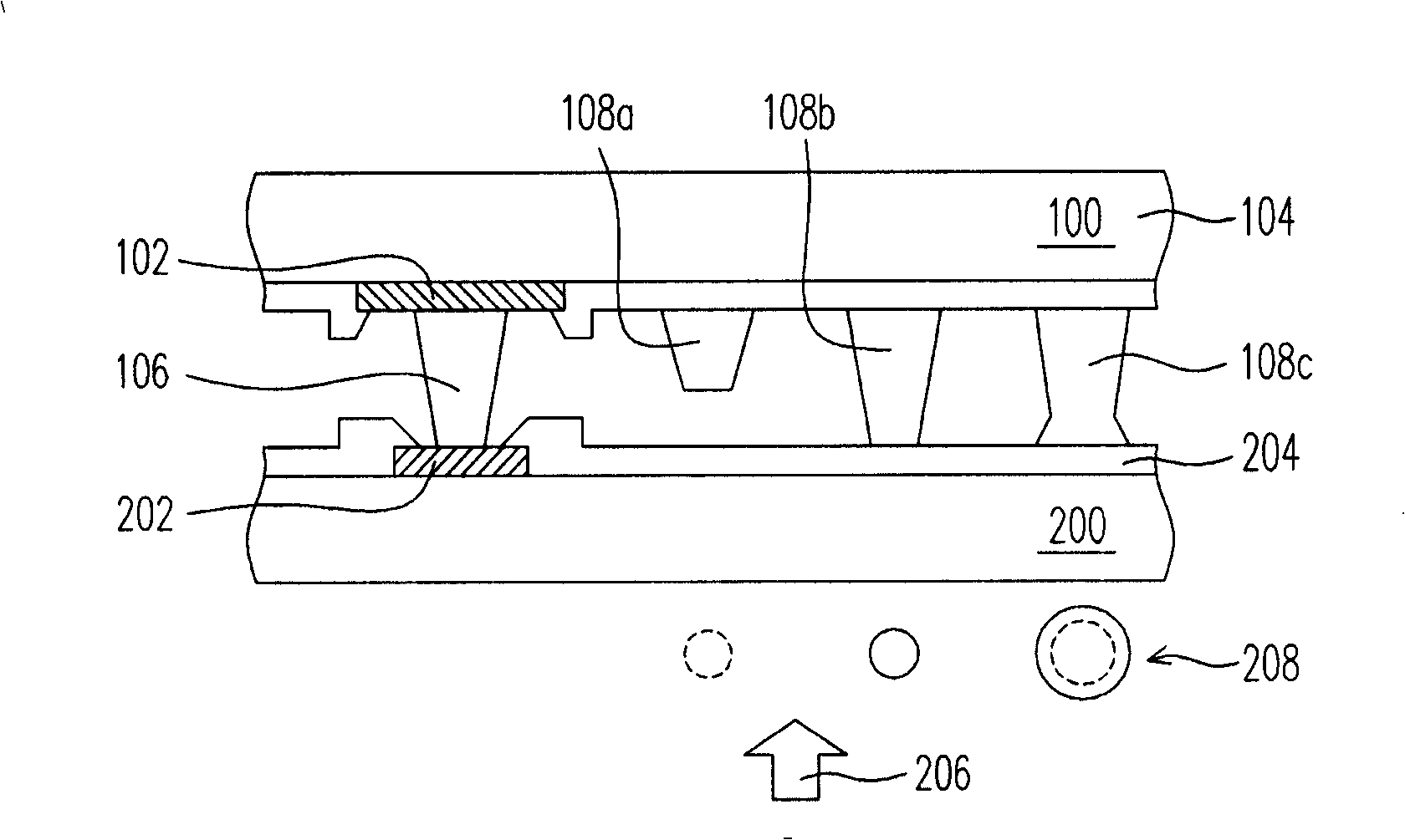
[0053] Figure 1A to Figure 1C is a schematic cross-sectional view of a bump structure on a substrate and its bonding process according to an embodiment of the present invention. Please refer to Figure 1A, the bump structure of this embodiment is configured on the substrate 100, which includes at least one electrode 102, a first bump 106, and second bumps 108a, 108b, 108c. In a preferred embodiment, the electrode 102 is formed on the substrate 100 , and a protective layer 104 is further formed on the surface of the substrate 100 , and the protective layer 104 exposes the electrode 102 . The substrate 100 is, for example, a silicon substrate, a glass substrate, a printed circuit board, a flexible substrate or a ceramic substrate. The material of the electrode 102 is metal, for example. In addition, the first bumps 106 are located on the electrodes 102 , and the second bumps 108 a , 108 b , 108 c are located on the substrate 100 , that is, the second bumps 108 a , 108 b , 108...
no. 2 example
[0066] Figure 8A to Figure 8C is a schematic cross-sectional view of a bump structure on a substrate and its bonding process according to an embodiment of the present invention. Please refer to Figure 8A , the bump structure of this embodiment is configured on the substrate 100 , which includes at least one electrode 102 and at least one stepped bump 306 . In a preferred embodiment, the electrode 102 is formed on the substrate 100 , and a protective layer 104 is further formed on the surface of the substrate 100 , and the protective layer 104 exposes the electrode 102 . In this embodiment, the stepped bump 306 is located on the electrode 102 . Similarly, the stepped bump 306 may be a metal bump, a conductive bump, or an elastic bump composed of a polymer bump and a conductive layer on the polymer bump. In addition, the transverse section of the stepped bump 306 is circular, elliptical, rectangular or polygonal. The stepped bump 306 is disposed on the electrode 102 or par...
PUM
 Abstract
Description
Claims
Application Information
 - R&D Engineer
- R&D Manager
- IP Professional
- Industry Leading Data Capabilities
- Powerful AI technology
- Patent DNA Extraction
Browse by: Latest US Patents, China's latest patents, Technical Efficacy Thesaurus, Application Domain, Technology Topic.
© 2024 PatSnap. All rights reserved.Legal|Privacy policy|Modern Slavery Act Transparency Statement|Sitemap