Supercharge Your Innovation With Domain-Expert AI Agents!

Method for manufacturing encoder substrate

A technology of an encoder and a manufacturing method, which is applied to electrical components, electrical switches, circuits, etc., can solve the problem that the surface of the conductive pattern 8 and the surface of the insulating plastic are prone to steps, the conductive pattern 8 is difficult to achieve in small intervals, and the shape of the model is difficult to achieve. complex issues

Inactive Publication Date: 2008-09-24
ALPS ALPINE CO LTD
View PDF1 Cites 4 Cited by
  • Summary
  • Abstract
  • Description
  • Claims
  • Application Information

AI Technical Summary

Problems solved by technology

[0009] As a result, in the manufacturing method described in Patent Document 1, it is difficult to achieve a small interval of the conductive pattern 8, and steps are likely to occur between the surface of the conductive pattern 8 and the surface of the insulating plastic, so there is a problem that it is difficult to form a smooth surface. The sliding surface problem
Since it is necessary to use another mold to injection mold the conductive plastic block 4 and the insulating plastic, and because the shape of the mold is also complicated, there are also problems of complicated manufacturing methods and high costs.

Method used


Image

  • Method for manufacturing encoder substrate
  • Method for manufacturing encoder substrate
  • Method for manufacturing encoder substrate

Examples


Embodiment Construction

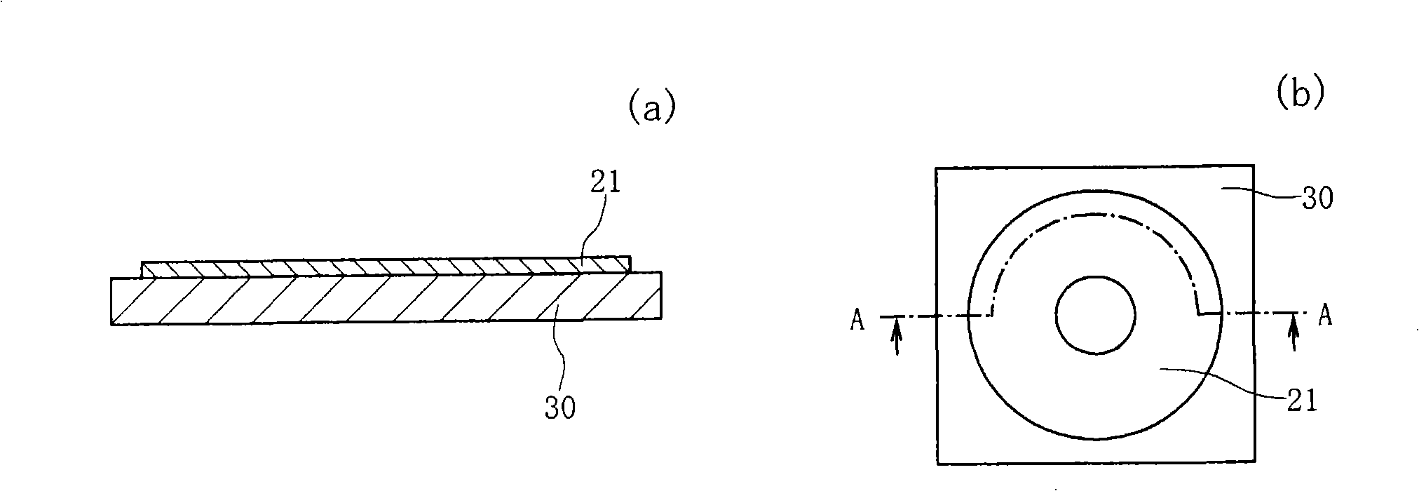
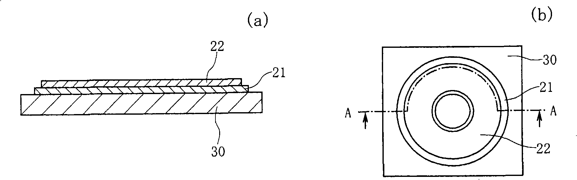
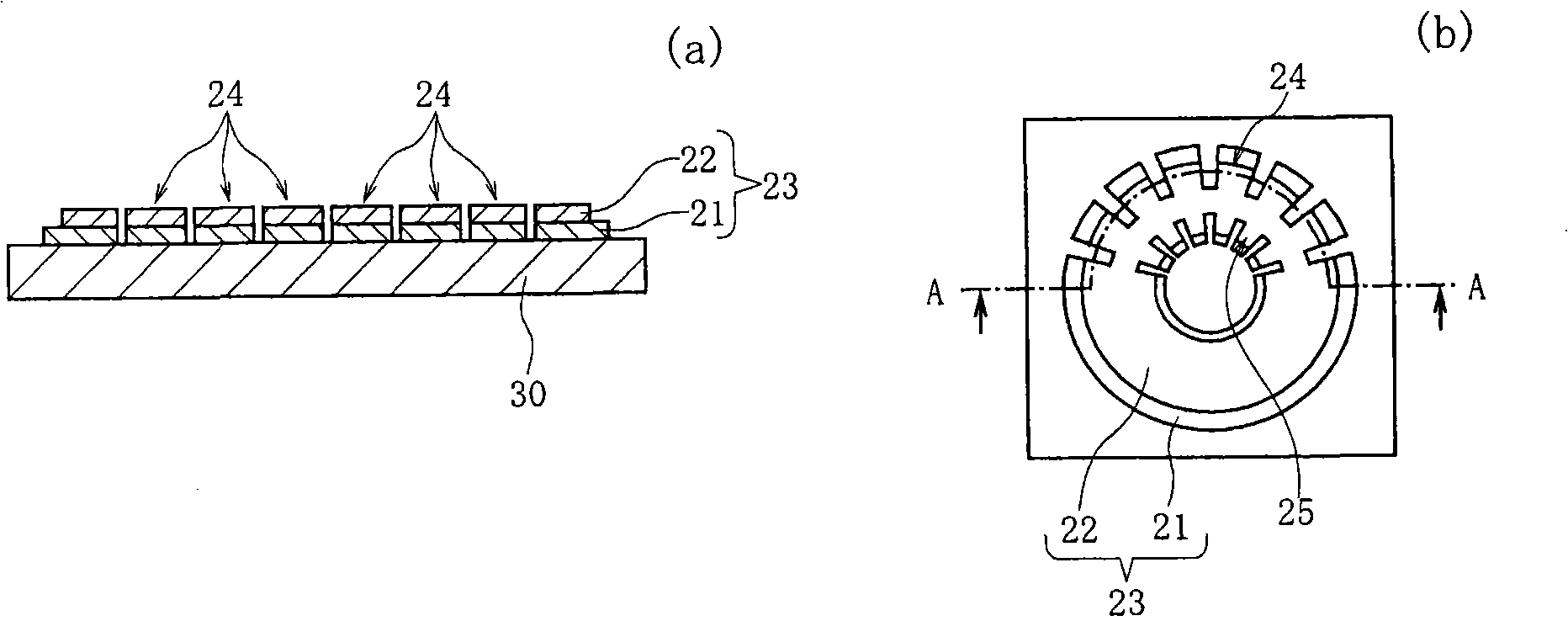
[0048] Figure 1 to Figure 6 A method of manufacturing the encoder substrate of this embodiment is shown. figure 1 (a), figure 2 (a), image 3 (a) and Figure 4 to Figure 6 It means that regardless of which process the above-mentioned encoder boards are used as figure 1 (b), figure 2 (b) and image 3 (b) The A-A line shown is cut along the film thickness direction, and the cross-sectional view seen from the direction of the arrow. figure 1 (b), figure 2 (b) and image 3 (b) is each figure 1 (a), figure 2 (a) and image 3 (a) Floor plan.

[0049] exist figure 1In the illustrated process, the first conductive layer 21 is formed by screen printing a first conductive paste on a transfer plate 30 made of, for example, a brass plate. The surface of the above-mentioned transfer plate 30 is given a mirror finish in advance. The above-mentioned transfer plate 30 is preferably made of metal. By forming the above-mentioned transfer plate 30 with metal, its thermal...


PUM


Abstract

The invention relates to a manufacturing method of a coder substrate, in particular to form a plurality of conductive parts in narrow interval with high precision, and form the surfaces of the conductive part and the insulating substrate smoothly at the same time, wherein the conductive paste with carbon powder and adhesive resin is printed on the transfer printing plate (30) to form the first conductive layer (21), the conductive paste with silver powder and adhesive resin is printed on the first conductive layer (21) to form the second conductive layer (22), and then the shape of the conductive layer (23) composed of the first conductive layer (21) and the second conductive layer (22) is processed by pictures, a first conductive part (24) is formed in the surrounding open interval of the conductive layer (23), and a second conductive part (25) is formed in the internal surrounding open interval. And then the conductive part is collocated in the mould, the insulating substrate composed of resin is shaped by injection, the interval between the conductive parts is filled with resin; at last, through peeling off the transfer printing plate (30), the conductive layer (23) is transferred to the insulating substrate side.

Description

technical field [0001] The present invention relates to a method of manufacturing an encoder substrate capable of forming a plurality of conductive portions at small intervals with high precision, and of smoothly forming the surfaces of the conductive portions and the surface of an insulating substrate. Background technique [0002] Patent Document 1 below discloses a method of manufacturing an encoder substrate. [0003] In the invention described in Patent Document 1, as described in columns (0014) to (0022) of Patent Document 1, first, a carbon paste film is formed by printing on the carrier film 1, and after the carbon layer 2 is formed by heating, the carrier The film 1 is arranged in a primary mold 3, and injection molding is performed on a block of conductive plastic. [0004] Next, the conductive plastic block 4 is taken out from the primary mold 3, and the carrier film 1 is peeled off. At this time, the carbon layer 2 is pattern-transferred onto the conductive pla...

Claims


Application Information

Patent Timeline
IPC IPC(8): H01H11/04
Inventor 小松寿
Owner ALPS ALPINE CO LTD
Features
  • R&D
  • Intellectual Property
  • Life Sciences
  • Materials
  • Tech Scout
  • Unparalleled Data Quality
  • Higher Quality Content
  • 60% Fewer Hallucinations
Learn More