Pixel structure and active element array substrate

A technology of active components and pixel structures, applied in the direction of electrical components, electrical solid-state devices, semiconductor devices, etc., can solve the problems of uneven etching of the gate insulating layer 50, poor characteristics of the storage capacitor C component, etc., so as to improve the display quality and avoid The effect of reducing the characteristics of the storage capacitor element and maintaining the aperture ratio

Active Publication Date: 2010-06-09
AU OPTRONICS CORP
View PDF0 Cites 0 Cited by
  • Summary
  • Abstract
  • Description
  • Claims
  • Application Information

AI Technical Summary

Problems solved by technology

However, this method easily makes the gate insulating layer 50 in the storage capacitor C face the problem of uneven etching, so that the element characteristics of the storage capacitor C are not good.

Method used


Image

  • Pixel structure and active element array substrate
  • Pixel structure and active element array substrate
  • Pixel structure and active element array substrate

Examples


Embodiment Construction

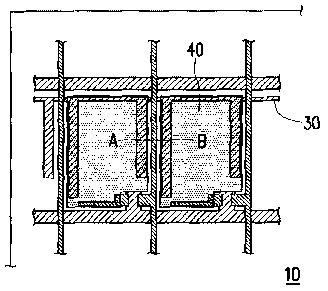
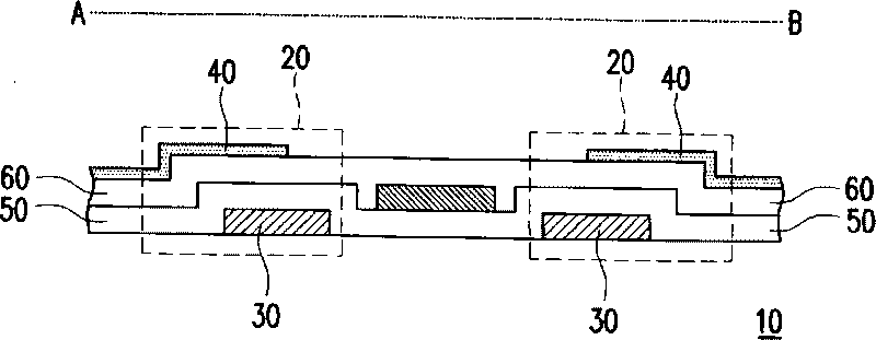
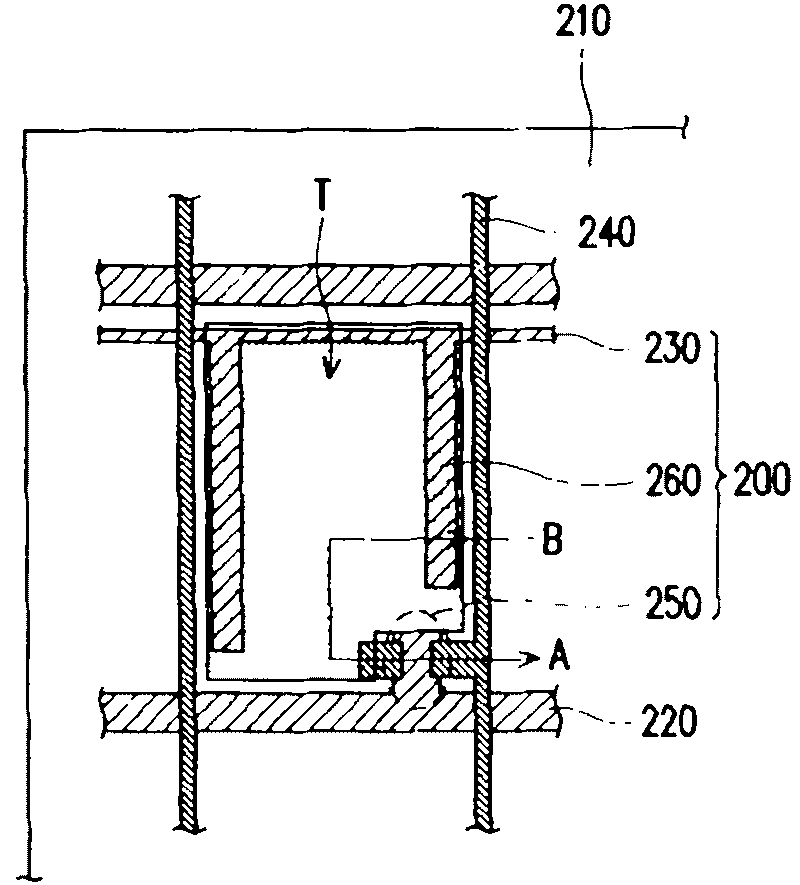
[0051] figure 2 is a schematic diagram of a pixel structure according to an embodiment of the present invention, and Figure 3A for figure 2 A schematic cross-sectional view of the pixel structure shown in , taken along the section line A-B. Please refer to figure 2 and Figure 3A , the pixel structure 200 of this embodiment is configured on a substrate 210, wherein the substrate 210 is, for example, a glass substrate, a plastic substrate or a substrate made of other materials. The pixel structure 200 is electrically connected to the scan line 220 and the data line 240, and the pixel structure 200 is mainly composed of an active element 250, a lower capacitor electrode 260, an insulating layer 270 and a pixel electrode 280. In this embodiment, the pixel structure 200 It also includes a shared wiring 230 , and the lower capacitor electrode 260 is a part of the shared wiring 230 .

[0052] Such as figure 2 and Figure 3A As shown, the active device 250 is driven by th...


PUM


Abstract

The invention relates to a pixel structure which is arranged on a baseplate and electrically connected with a scan line and a data line. The pixel structure comprises an active element, a lower capacitor electrode, an insulation layer and a pixel electrode. The active element is arranged on the baseplate, wherein, the active element is provided with a grid, a source electrode and a drain electrode, and the active element is electrically connected with the scan line and the data line. The lower capacitor electrode and the grid are separately arranged on the baseplate. The insulation layer covers the active element and the lower capacitor electrode, wherein, the insulation layer consists of a single film layer. The pixel electrode is electrically connected with the active element, and at least partial pixel electrode extends to the insulation layer on the upper part of the lower capacitor electrode.

Description

technical field [0001] The invention relates to a pixel and a liquid crystal display panel, and in particular to a pixel structure with a storage capacitor and an active element array substrate. Background technique [0002] Liquid crystal displays have the advantages of high image quality, small size, light weight, low voltage drive, low power consumption, and wide application range. Therefore, they have replaced cathode ray tubes (Cathode Ray Tube, CRT) and become the mainstream of the new generation of displays. Generally speaking, a liquid crystal display panel is mainly composed of an active element array substrate, a color filter substrate and a liquid crystal layer. [0003] More specifically, the active element array substrate is composed of a plurality of thin film transistors arranged in an array and pixel electrodes corresponding to each thin film transistor, wherein the thin film transistors are used as switching elements of the liquid crystal display unit. In a...

Claims


Application Information

Patent Timeline
Patent Type & Authority Patents(China)
IPC IPC(8): H01L23/522G02F1/1362H01L27/12
Inventor 廖信铭黄国有林汉涂
Owner AU OPTRONICS CORP
Why Eureka
Try Eureka