Electronic device or circuit and method for fabricating the same

A technology for electronic devices and circuits, which is applied in the manufacture of printed circuits, printed circuits and electrical components connected with non-printed electrical components, and can solve problems such as high device costs.

Inactive Publication Date: 2008-10-15
NXP BV
View PDF1 Cites 15 Cited by
  • Summary
  • Abstract
  • Description
  • Claims
  • Application Information

AI Technical Summary

Problems solved by technology

[0006] The problem with the application of these types of electronic devices is that the cost of these devices (which are

Method used


Image

  • Electronic device or circuit and method for fabricating the same
  • Electronic device or circuit and method for fabricating the same
  • Electronic device or circuit and method for fabricating the same

Examples


Embodiment Construction

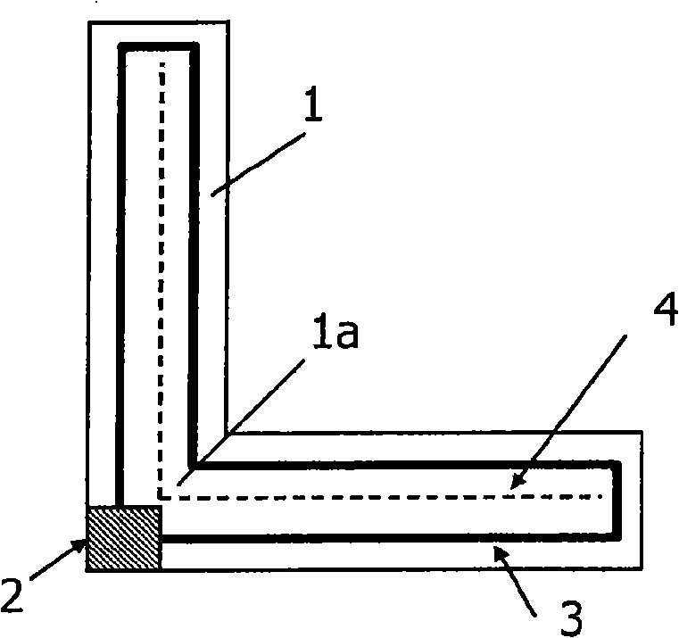
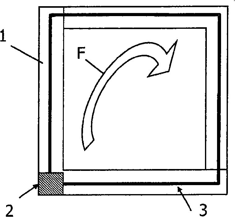
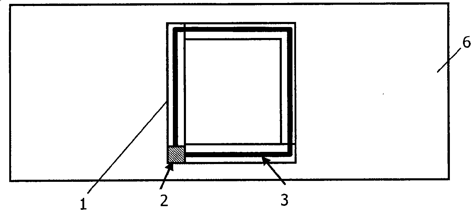
[0038] The present invention will now be described in terms of various embodiments that facilitate the fabrication of electronic devices or circuits, such as integrated electronic systems or passive electronic components, that are distributed over an area much larger than the actual substrate on which they are fabricated. explained. In this way, device sensitivity is increased while keeping cost price low. Electronic devices and circuits are implemented in flexible substrates using a cut-fold-extend method based on electronic technologies such as low temperature polysilicon (LTPS). It is known that LTPS can be realized on flexible substrates by fabricating the LTPS directly on a thin plastic or metal substrate, or alternatively by transferring the LTPS from the (glass) substrate on which it is fabricated to a flexible substrate. Using this technique, the inventors intend to create distributed electronic systems with built-in interconnect lines for input (sensors) and output (...


PUM


Abstract

A method for fabricating an electronic device or circuit, respectively, comprises providing a flexible substrate (1), defining onto the flexible substrate (1) electric components (2, 3, 3', 3'', 3''', 7, 11, 12) and interconnects (8), introducing out breaks (4, 4', 4'', 4a-4s) in the flexible substrate (1) between the electric components and/or interconnects, and forming the flexible substrate (1) into a deformed configuration by deforming, particularly folding, parts of the flexible substrate as determined by the breaks (4, 4', 4'', 4a-4s).

Description

technical field [0001] The invention relates to a method for manufacturing an electronic device or circuit, respectively, comprising providing a flexible substrate, and defining electronic components and interconnection lines on the flexible substrate. [0002] The invention also relates to electronic devices or circuits, respectively, comprising a flexible substrate on which electronic components and interconnections are defined. Background technique [0003] In many cases, the cost of electronic devices or circuits scales linearly with the area of ​​the substrate on which they are fabricated. Consequently, many products benefit from reduced cost of components miniaturization and efficient packaging of components, for example on printed circuit boards (PCBs). However, it should be noted that the miniaturization of components and efficient packaging of these components requires the use of expensive multilayer PCBs and the application of multilayer fabrication techniques. O...

Claims


Application Information

Patent Timeline
IPC IPC(8): H05K1/00H05K1/18
CPCH05K1/189H05K1/028H05K3/0058H05K3/281H05K2201/052H05K2201/055
Inventor 马克・T・约翰逊阿德里安努斯・森珀尔弗朗西斯库斯・P・威德肖温
Owner NXP BV
Why Eureka
Try Eureka