

Test substrate, test substrate mask and test substrate forming method
A mask pattern and substrate technology, which is applied in the field of integrated circuit manufacturing, can solve the problems of lack of passivation layer, deterioration of isolation effect of shallow trench isolation area, and reduction of height difference, so as to improve authenticity and suppress the phenomenon of passivation layer loss Effect
Inactive Publication Date: 2008-10-29
SEMICON MFG INT (SHANGHAI) CORP
View PDF2 Cites 0 Cited by
- Summary
- Abstract
- Description
- Claims
- Application Information
AI Technical Summary
Problems solved by technology
However, in production practice, when the passivation layer is used as a polishing stop layer to planarize the shallow trenches after filling spacers, if the size of the passivation layer is the same as that in the adjacent shallow trenches If the size difference of the filling spacer is too large, it is easy to cause the lack of the passivation layer, so that the height difference between the surface of the shallow trench isolation region and the surface of the active region isolated by it is reduced, and the reduced height difference is not enough Eliminate the gap between the shallow trench isolation region and the semiconductor substrate, that is, the reduced height difference will easily lead to the deterioration of the isolation effect of adjacent shallow trench isolation regions
Method used
View moreImage
Smart ImageViewing Examples

Examples
Embodiment Construction
Login to View More PUM
 Abstract
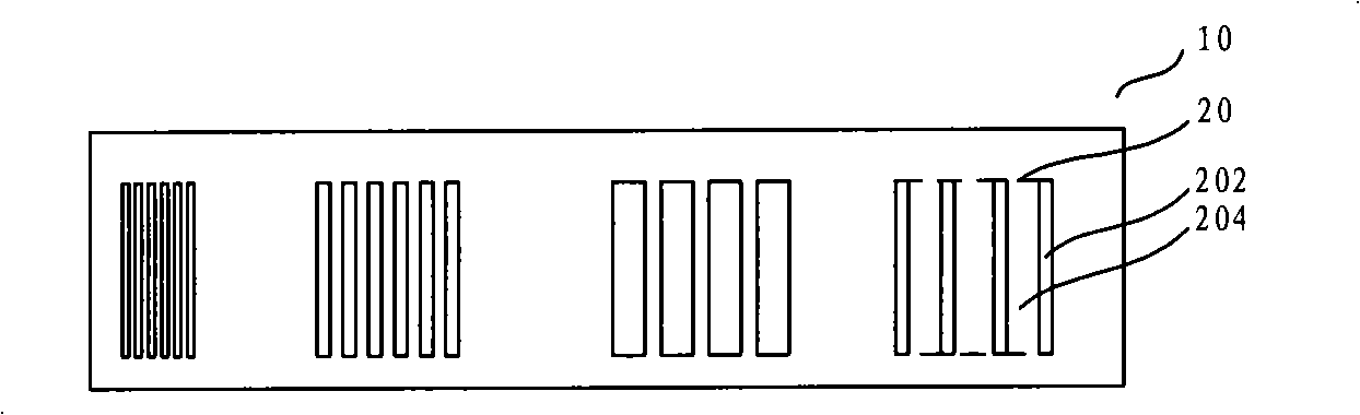
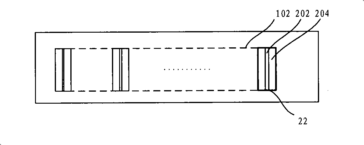
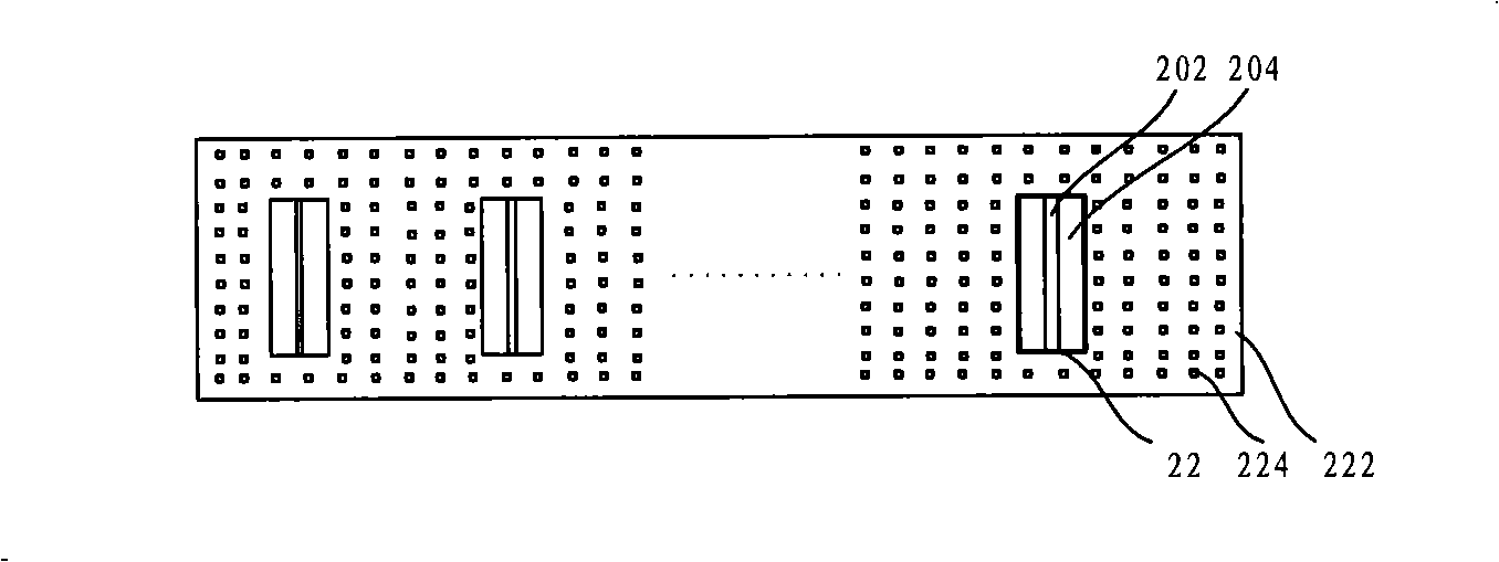
A test matrix comprises at least one independent test unit series; the single independent test unit series comprises at least two independent test units; the independent test unit comprises a basic test element and two auxiliary basic test elements; the basic test element is connected with the auxiliary basic test elements by alternation. The invention also provides a test matrix mask and a forming method of the test matrix. A proper technique window can be obtained by testing the change of the losing of a passivation layer so as to restrain the losing phenomenon of the passivation layer from being generated.
Description
Method for forming test substrate, test substrate mask and test substrate technical field The invention relates to the technical field of integrated circuit manufacturing, in particular to a test base, a test base mask and a method for forming the test base. Background technique In the traditional integrated circuit manufacturing process, in order to ensure the quality of the product, inspection is required after many steps involved in the manufacturing process, such as inspection of products after grinding or etching. Usually, a test matrix is fabricated on a semiconductor substrate, and then the test matrix is used to replace the product for testing. In order to enable the test base to truly simulate the relevant manufacturing process of the product, the test base and the product are produced synchronously. Various attempts have been made in the industry regarding the structure of the test base and how to use the test base to perform process inspection and then com...
Claims
Login to View More Application Information
Patent Timeline
 IPC IPC(8): H01L23/544H01L21/00G03F1/14G03F1/44
Inventor邓永平
OwnerSEMICON MFG INT (SHANGHAI) CORP