

Display panel and optoelectronic device
A technology for display panels and substrates, applied in lighting devices, optics, light sources, etc., can solve problems such as compressing the layout space of wire structures
- Summary
- Abstract
- Description
- Claims
- Application Information
AI Technical Summary
Problems solved by technology
Method used
Image

Examples
Embodiment Construction
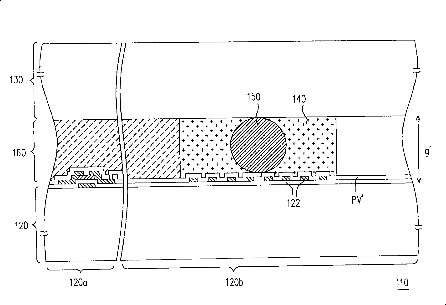
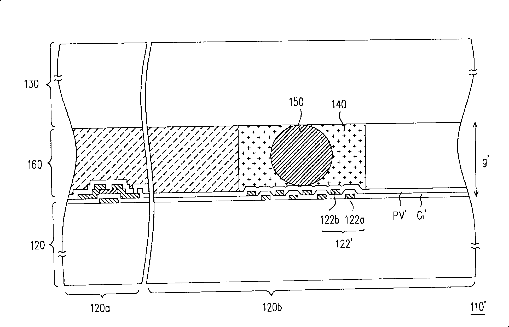
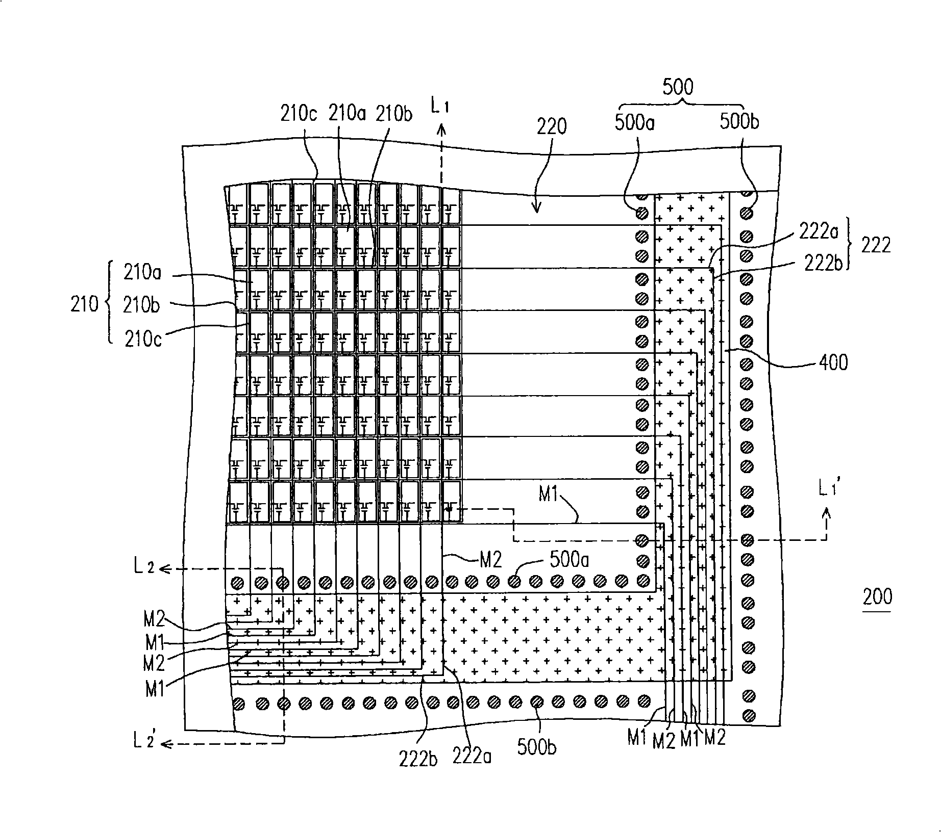
[0043] figure 2 A partial top view of a display panel according to an embodiment of the present invention is shown. Figure 2A based on figure 2 The sectional view along the section line L1-L1' in the middle. in, figure 2 Only part of the first substrate 200 in the display panel 100 is shown. Please refer to the same time figure 2 and Figure 2A , the display panel 100 of this embodiment includes a first substrate 200 , a second substrate 300 , a sealant 400 , a plurality of supports 500 and a display medium layer 600 .
[0044] The first substrate 200 has a pixel array 210 and peripheral lines 220 connected to the pixel array 210 .
[0045] The second substrate 300 is disposed above the first substrate 200 .
[0046] The sealant 400 is disposed between the first substrate 200 and the second substrate 300 , and the sealant 400 is located on a portion of the peripheral circuit 220 and surrounds the pixel array 210 . The peripheral circuit 200 has a multi-layer wire ...
PUM
 Abstract
Description
Claims
Application Information