Liquid crystal display device and image display method thereof
A liquid crystal display device and image display technology, applied to static indicators, instruments, etc., can solve the problems of reducing power consumption and being unable to adopt, and achieve the effects of reducing power consumption, improving quality, and suppressing the deviation of brightness or color tone
- Summary
- Abstract
- Description
- Claims
- Application Information
AI Technical Summary
Problems solved by technology
Method used
Image

Examples
no. 1 approach
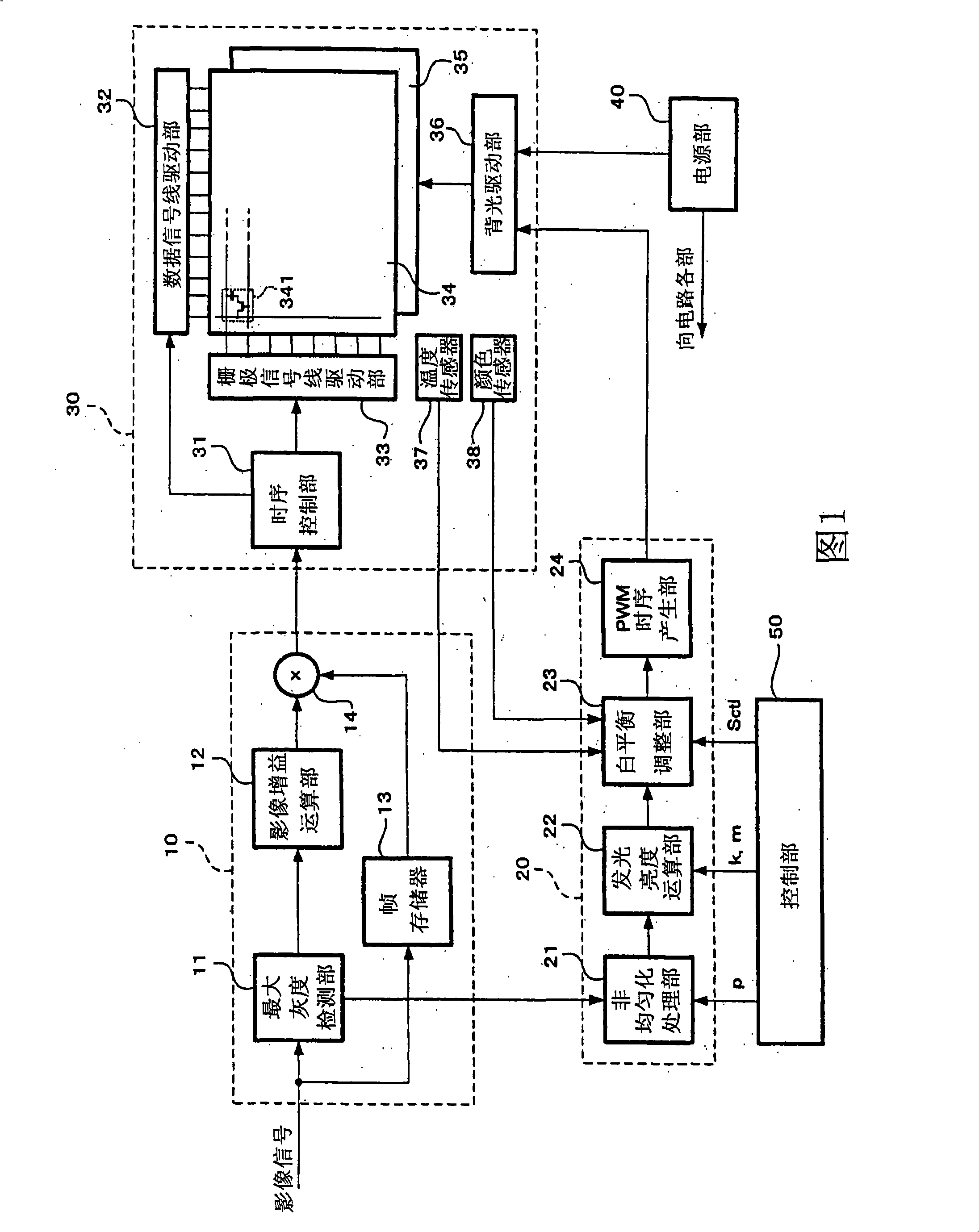
[0068] Hereinafter, a liquid crystal display device according to a first embodiment of the present invention and an image display method used in the device will be described with reference to the drawings. FIG. 1 is a block diagram showing the overall configuration of a liquid crystal display device according to Embodiment 1 of the present invention. In FIG. 1 , video signals displayed on a liquid crystal panel 34 in a liquid crystal module unit 30 described later are supplied to a maximum grayscale detection unit 11 and a frame memory 13 in a video signal processing unit 10 . As will be described later, the backlight device 35 is divided into a plurality of regions, and the liquid crystal panel 34 is divided into a plurality of regions corresponding to each region of the backlight device 35. For each region of the liquid crystal panel 34, the brightness (the amount of light) of the backlight ) are controlled separately.
[0069] figure 2 It is an example of area division on...
no. 2 approach
[0124] 21 is a block diagram showing an overall configuration of a liquid crystal display device according to a second embodiment of the present invention. In FIG. 21, the same parts as those in FIG. 1 are given the same reference numerals, and description thereof will be appropriately omitted. In addition, in FIG. 21 , the non-uniformization processing unit 21 in FIG. 1 is omitted for simplification, but a configuration having the non-uniformization processing unit 21 may also be used as in the first embodiment.
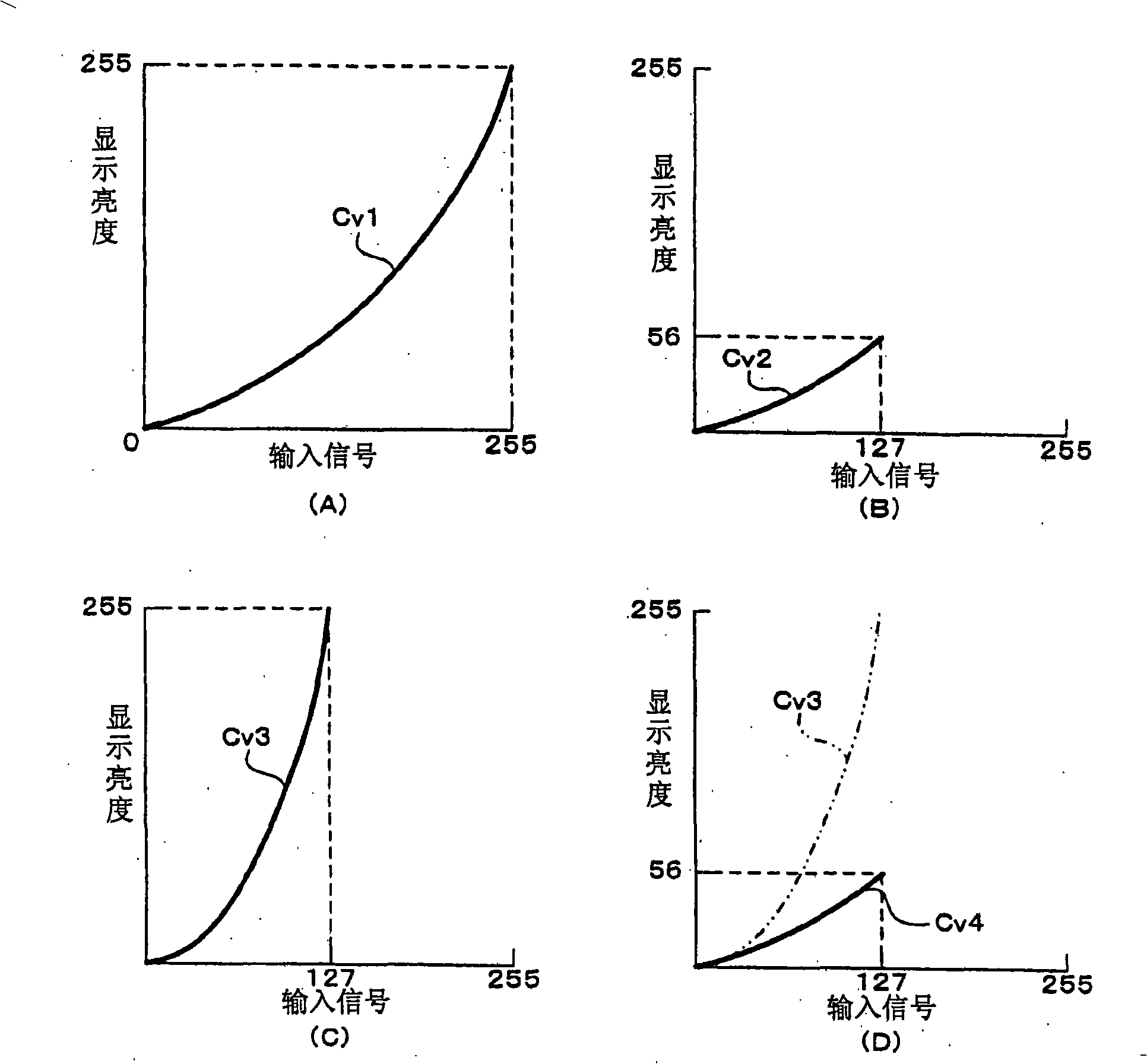
[0125] As described above, in the first embodiment, the light emission luminance Bo of light to be emitted by the light sources 352 in the plurality of regions of the backlight device 35 is obtained from the emission luminance calculation unit 22 to make the light sources 352 in the plurality of regions emit light. The luminance Bo is the luminance value at the center point of each area. Figure 22 (A) indicates that only the backlight device 35 such as Figure 4 ...
no. 3 approach
[0132] 26 is a block diagram showing the overall configuration of a liquid crystal display device according to Embodiment 3 of the present invention. In FIG. 26, the same parts as those in FIG. 1 are given the same reference numerals, and description thereof will be appropriately omitted. In addition, in FIG. 26 , the non-uniformization processing unit 21 in FIG. 1 is omitted for simplification, but a configuration having the non-uniformization processing unit 21 may also be used as in the first embodiment. In addition, in FIG. 26, although the light emission amount calculation part 25 is the same as that of 2nd Embodiment, the structure which removes the light emission amount calculation part 25 may be sufficient.
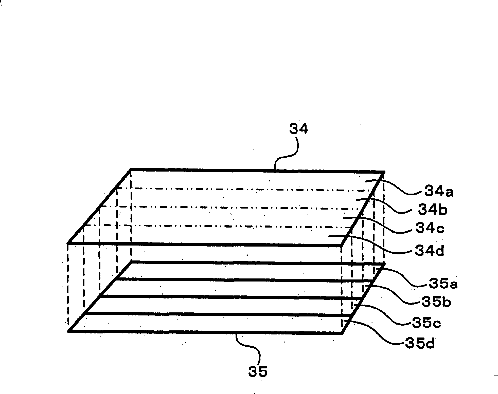
[0133] 27(A) is a situation where the liquid crystal panel 34 is divided into areas 34a-34d corresponding to the areas 35a-35d of the backlight device 35A, showing that the gray scale of the areas 34a, 34b, and 34d is 0 (that is, black) and the area 34c is The ca...
PUM
 Abstract
Description
Claims
Application Information
 - R&D
- Intellectual Property
- Life Sciences
- Materials
- Tech Scout
- Unparalleled Data Quality
- Higher Quality Content
- 60% Fewer Hallucinations
Browse by: Latest US Patents, China's latest patents, Technical Efficacy Thesaurus, Application Domain, Technology Topic, Popular Technical Reports.
© 2025 PatSnap. All rights reserved.Legal|Privacy policy|Modern Slavery Act Transparency Statement|Sitemap|About US| Contact US: help@patsnap.com