Semiconductor device
A semiconductor and device technology, applied in the field of semiconductor devices
- Summary
- Abstract
- Description
- Claims
- Application Information
AI Technical Summary
Problems solved by technology
Method used
Image

Examples
Embodiment Construction
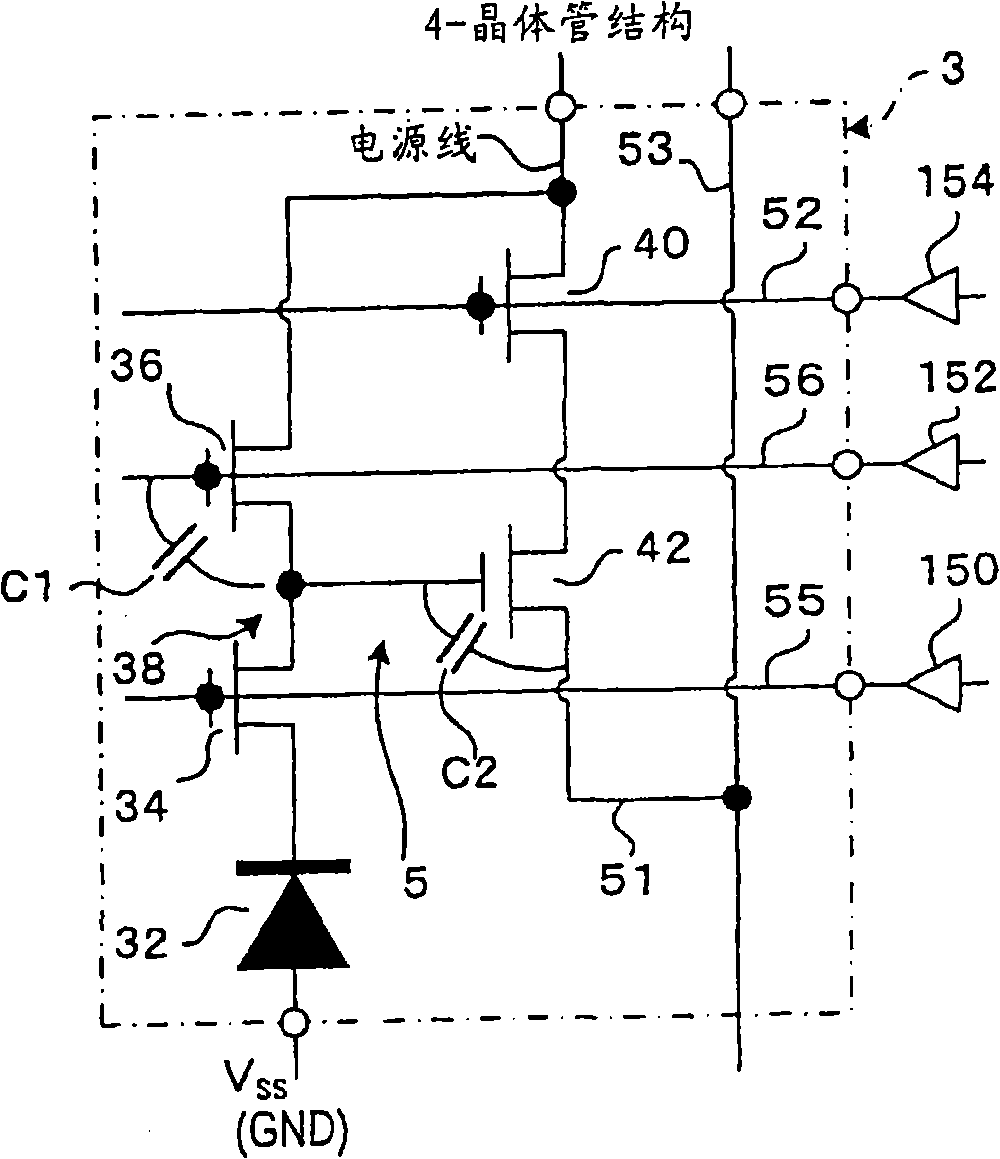
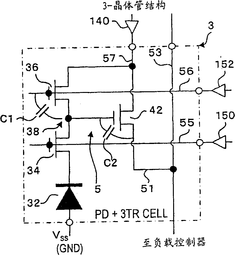
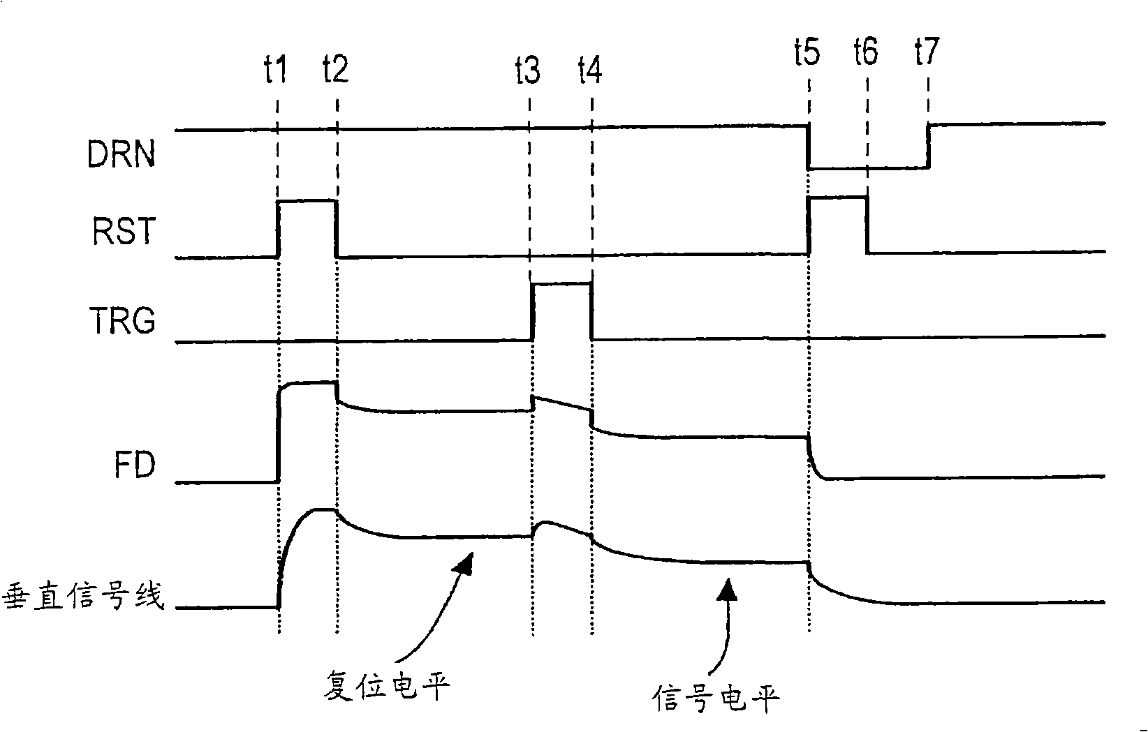
[0055] Hereinafter, embodiments of the present invention will be described in detail with reference to the accompanying drawings. Hereinafter, an embodiment of a device using a CMOS imaging sensor, which is an example of an X-Y address type solid-state imaging device, will be described. Also, all pixels of the CMOS imaging sensor are composed of NMOS. However, this is only an example. The device is not limited to a MOS type imaging device. All the embodiments described below apply to all physical quantity distribution sensing semiconductor devices in which a plurality of unit components are sensitive to externally input electromagnetic waves such as light and rays and are arranged in a row or in a matrix. Also, it should be noted that in the embodiment according to the present invention, the words "row" and "column" used for the pixel arrangement and the direction of the line represent the horizontal direction and the vertical direction of the matrix, respectively. However,...
PUM
 Abstract
Description
Claims
Application Information
 - R&D Engineer
- R&D Manager
- IP Professional
- Industry Leading Data Capabilities
- Powerful AI technology
- Patent DNA Extraction
Browse by: Latest US Patents, China's latest patents, Technical Efficacy Thesaurus, Application Domain, Technology Topic.
© 2024 PatSnap. All rights reserved.Legal|Privacy policy|Modern Slavery Act Transparency Statement|Sitemap