

Probe apparatus
A detection device and detection card technology, applied in the direction of measuring devices, measuring electricity, measuring electrical variables, etc., can solve the problems of increased occupied area, hard work, high efficiency of wafer transfer, etc., and achieve the effect of reducing standby time and improving productivity
Inactive Publication Date: 2008-11-19
TOKYO ELECTRON LTD
View PDF2 Cites 15 Cited by
- Summary
- Abstract
- Description
- Claims
- Application Information
AI Technical Summary
Problems solved by technology
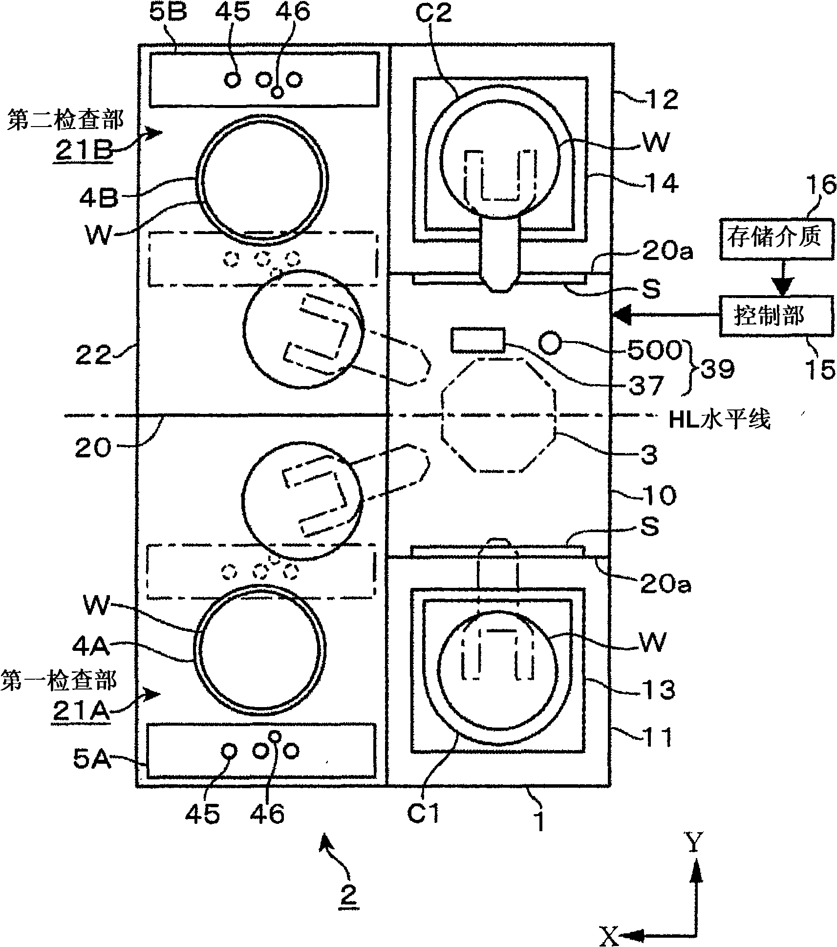
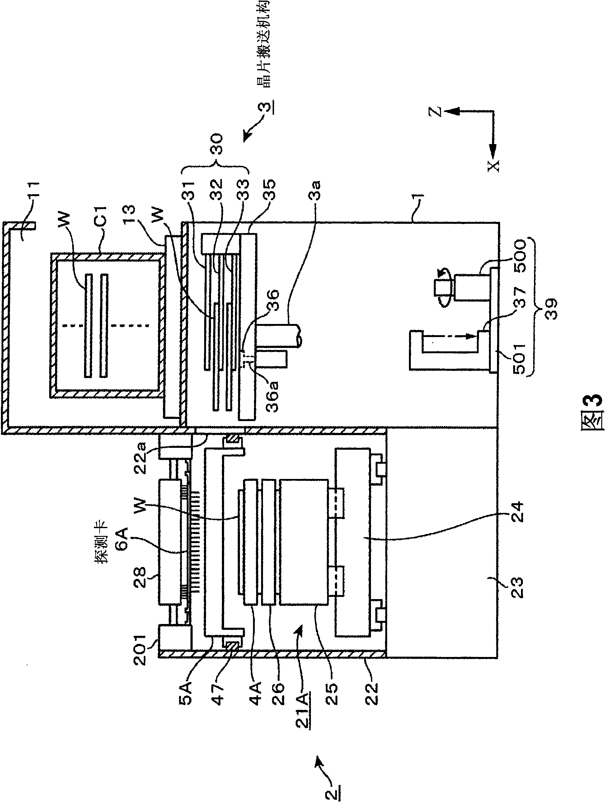
However, since the inspection unit itself has not worked hard on miniaturization, the area occupied by the device is increased by installing the inspection unit on both sides of the loading unit. The transfer tweezers that can move forward and backward along the length direction of the loading section and the two swing arms that transfer wafers between the tweezers and the left and right inspection sections, so it is difficult to say that the wafer transfer efficiency is high, and because these swing arms must be secured Therefore, it cannot solve the problem of miniaturization of the whole device
Method used
View moreImage
Smart ImageViewing Examples


Examples
no. 1 Embodiment approach
no. 2 Embodiment approach
Login to View More PUM
 Abstract
The invention provides a probe apparatus. The apparatus uses the probe card to invest the electrical characteristics of IC chip on wafer to improve the transferring efficiency and realize high production efficiency. The probe apparatus is provided with a load port for mounting therein a carrier having therein a plurality of substrates; a plurality of probe apparatus main bodies, each having a probe card having probes on its bottom surface; a substrate transfer mechanism for transferring the substrates between the load port and the probe apparatus main bodies, the substrate transfer mechanism being rotatable about a vertical axis and movable up and down. The substrate transfer mechanism has at least three substrates capable of moving back and forth independently. Further, at least two wafers are received from the carrier by the substrate transfer mechanism, and then are sequentially loaded into the probe apparatus main bodies.
Description
detection device technical field The present invention relates to a technique for measuring electrical characteristics of an object to be inspected by bringing a probe into electrical contact with electrode pads of the object to be inspected. Background technique After an IC chip is formed on a semiconductor wafer (hereinafter referred to as wafer), in order to investigate the electrical characteristics of the IC chip, a probe test is performed by a probe device in the state of the wafer. If the flow of the wafer in this detecting device is simply described, firstly, the wafer is taken out from the carrier accommodating a plurality of wafers by the transfer mechanism, and the positioning process called the pre-alignment process and the acquisition process called the OCR process are performed on the wafer. Processes such as ID etc. formed on the wafer. Then, the wafer is carried into the detector body, and the wafer is placed on a wafer chuck that is free to move along the...
Claims
Login to View More Application Information
Patent Timeline
 Patent Type & AuthorityApplications(China)
IPC IPC(8): G01R31/28G01R1/02
CPCG01R1/07307G01R3/00G01R31/2601H01L22/30
Inventor带金正秋山收司
OwnerTOKYO ELECTRON LTD