Site yield statistical method for multi-site parallel test

A statistical method and yield rate technology, applied to electrical components, semiconductor/solid-state device manufacturing, circuits, etc., can solve the problems of reducing test efficiency, affecting test output, prolonging downtime, etc., to save standby time and improve test production efficiency , the effect of reducing the floor area

Inactive Publication Date: 2011-10-12
BEIJING CHIPADVANCED
View PDF0 Cites 12 Cited by
  • Summary
  • Abstract
  • Description
  • Claims
  • Application Information

AI Technical Summary

Problems solved by technology

These test information are all for the detection of the chip itself. However, when the chip test results fail due to non-chip internal failures, it is difficult to determine which factors cause the chip failure. The usual methods are shutdown, Interrupt the test process, software engineers and hardware engineers analyze the reasons together, us

Method used


Image

  • Site yield statistical method for multi-site parallel test
  • Site yield statistical method for multi-site parallel test
  • Site yield statistical method for multi-site parallel test

Examples


Embodiment Construction

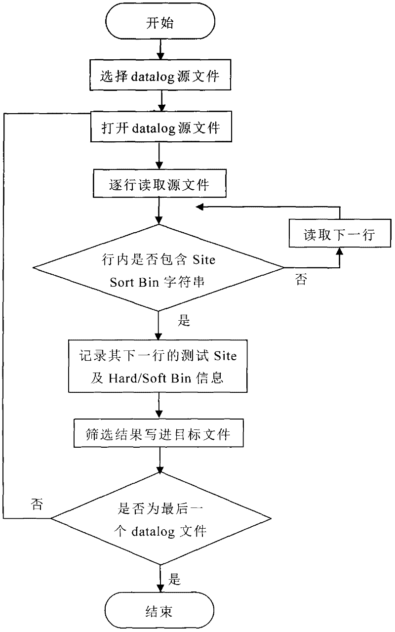
[0025] The method of the present invention is described in detail below by example:

[0026] Take out the number of Bin values ​​in each site from the test data, especially the proportion of Bin 1, such as figure 1 shown.

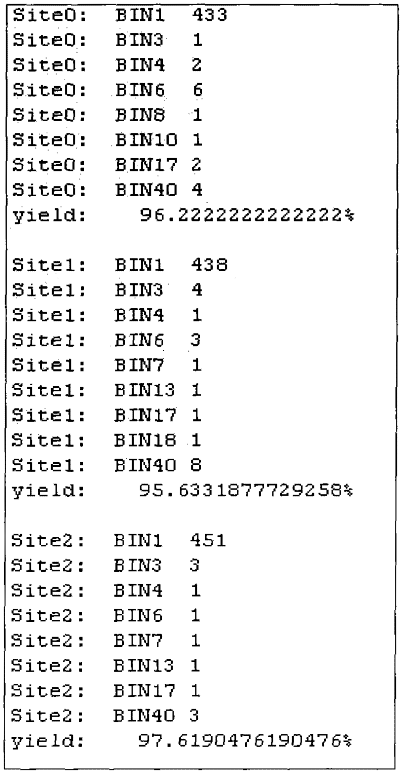
[0027] After the statistical software designed in this step runs, the information contained in the generated file includes Site, bin value and its quantity, and the proportion of bin1 in the site test; figure 2 shown.

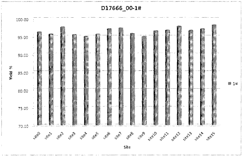
[0028] Draw a histogram according to the proportion of Bin 1 in each site test result, so that you can intuitively compare all sites horizontally. image 3 It is the yield histogram obtained from the statistics of 16site parallel test results. The horizontal axis is the site, and the vertical axis is the yield of each site.

[0029] There is a certain gap between the yield rates of each site. The reasons for these gaps are not only factors such as the random distribution of the chip itself, but also the test hardware that more or less a...


PUM


Abstract

The invention discloses a method for determining the state of testing hardware by using statistical test data in the process of testing a wafer of an integrated circuit. The test data generated in the process of testing the wafer reflects the physical parameter of each chip, the function of an internal module, a manufacturing process of each chip, and the state of the testing hardware in the testing process. By a site yield statistical method for a multi-site parallel test, whether the state of the testing hardware in the testing process is defective or not is checked. By the method, the yield of each site is obtained through the statistical induction of massive test data, and specific bin value distribution is obtained, so that the failure cause of the testing hardware can be quickly found, solution measures are taken, and test quality is ensured.

Description

technical field [0001] The invention relates to a method for detecting equipment status by using statistical test data in the process of testing an integrated circuit wafer, and belongs to the technical field of integrated circuit testing. Background technique [0002] At present, in the process of developing new products, especially in mass production, chip design companies and testing factories mainly judge whether the physical parameters and module functions inside the chip are good or not based on the massive data generated during the testing process, and further confirm the wafer manufacturing process. Whether the process or packaging process meets the design requirements. These test information are all for the detection of the chip itself. However, when the chip test results fail due to non-chip internal failures, it is difficult to determine which factors cause the chip failure. The usual methods are shutdown, Interrupt the test process, software engineers and hardwa...

Claims


Application Information

Patent Timeline
IPC IPC(8): H01L21/00
Inventor 金兰石志刚吉国凡张琳佘博文王慧孙昕
Owner BEIJING CHIPADVANCED
Why Eureka
Try Eureka