
Photoconductive device

An electrode, semiconductor technology, applied in the direction of semiconductor devices, electrical components, circuits, etc., can solve problems such as configuration limitations

Inactive Publication Date: 2011-04-13
PICOMETRIX
View PDF0 Cites 0 Cited by
  • Summary
  • Abstract
  • Description
  • Claims
  • Application Information

AI Technical Summary

Problems solved by technology

The problem, however, is that such semiconductors, like all narrowing bandgap semiconductors, are severely limited in their configuration as photoconductive switches.

Method used


Image

  • Photoconductive device
  • Photoconductive device
  • Photoconductive device

Examples


Embodiment Construction

[0019] Although it looks similar in function to a photodiode, the photoconductive switch is different in the following main aspects:

[0020] 1. The response time of the photoconductive switch can be mainly determined by the carrier lifetime of the semiconductor rather than by the applied electric field that depends on the geometry as in the photodiode. This means that a photoconductive switch with a gap of 1 μm can have a sub-picosecond lifetime, while the response time of a photodiode with a similar structure is several picoseconds. This also means that its response time does not depend on the applied electric field. The response time of a photoconductor with a fast carrier lifetime and a 1mV bias applied to the gap is the same as that of a photoconductor with a 1V bias.

[0021] 2. The applied electric field across the photoconductive switch affects the generated photoelectric flux. In contrast, the voltage across the photodiode has almost no effect on the photoelectric flux. ...


PUM


Abstract

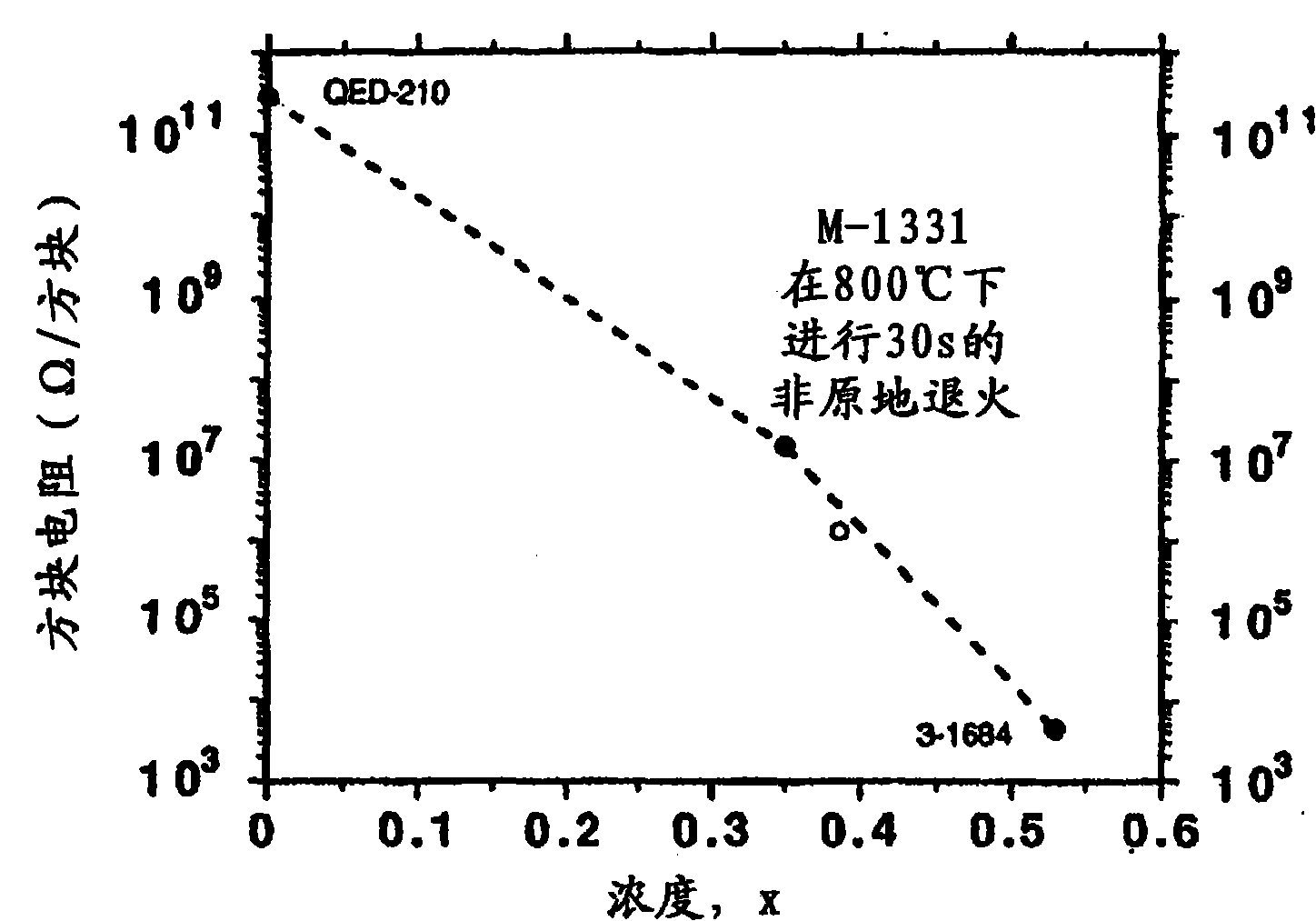
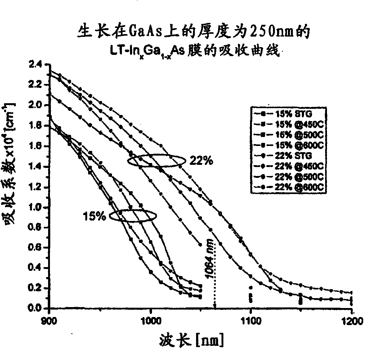
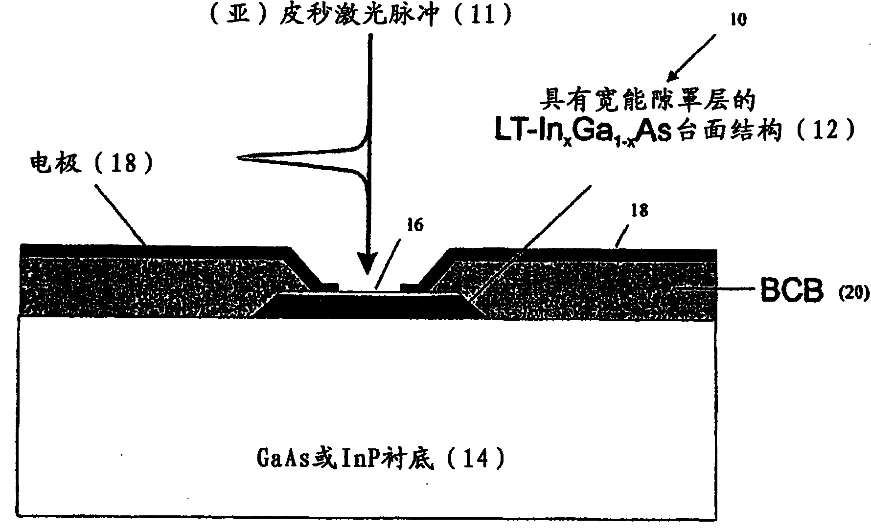
A semiconductor structure includes a GaAs or InP substrate, an InxGa1-xAs epitaxial layer grown on the substrate, where x is greater than about 0.01 and less than about 0.53, and a wider bandgap epitaxial layer grown as a cap layer on top of the InxGa1-xAs epitaxial layer.

Description

[0001] Related application [0002] This application claims the priority of U.S. Provisional Patent Application No. 60 / 633,862, the filing date of which is December 7, 2004, and the entire contents of which are incorporated herein by reference. Technical field [0003] The present invention relates to epitaxial growth type semiconductors. Background technique [0004] In order to generate picosecond or subpicosecond electrical transients by laser pulses, special processed semiconductors need to be used, and the most suitable is low temperature growth GaAs (LT-GaAs). A photoconductive switch based on this material can respond quickly to short laser pulses and can generate fast electrical transients when configured as a pulse generator. It can also be configured as a sampling gate to sample and measure short (picosecond) segments of unknown radio waves. It is the essence of sampling oscilloscopes to reconstruct and display the shape of the electric wave by sequentially sampling all ...

Claims


Application Information

Patent Timeline
Patent Type & Authority Patents(China)
IPC IPC(8): H01L31/09
CPCH01L31/09H01L31/03046H01L29/7371
Inventor 罗伯特·N·萨克斯马修·M·加兹维耶基斯蒂文·L·威廉姆森
Owner PICOMETRIX
Learn More