Method and device for optimizing chip layout of silicon slice
A chip layout, silicon wafer technology, applied in instrumentation, computing, electrical digital data processing, etc., can solve problems such as unreasonable chip layout
- Summary
- Abstract
- Description
- Claims
- Application Information
AI Technical Summary
Problems solved by technology
Method used
Image

Examples
Embodiment Construction
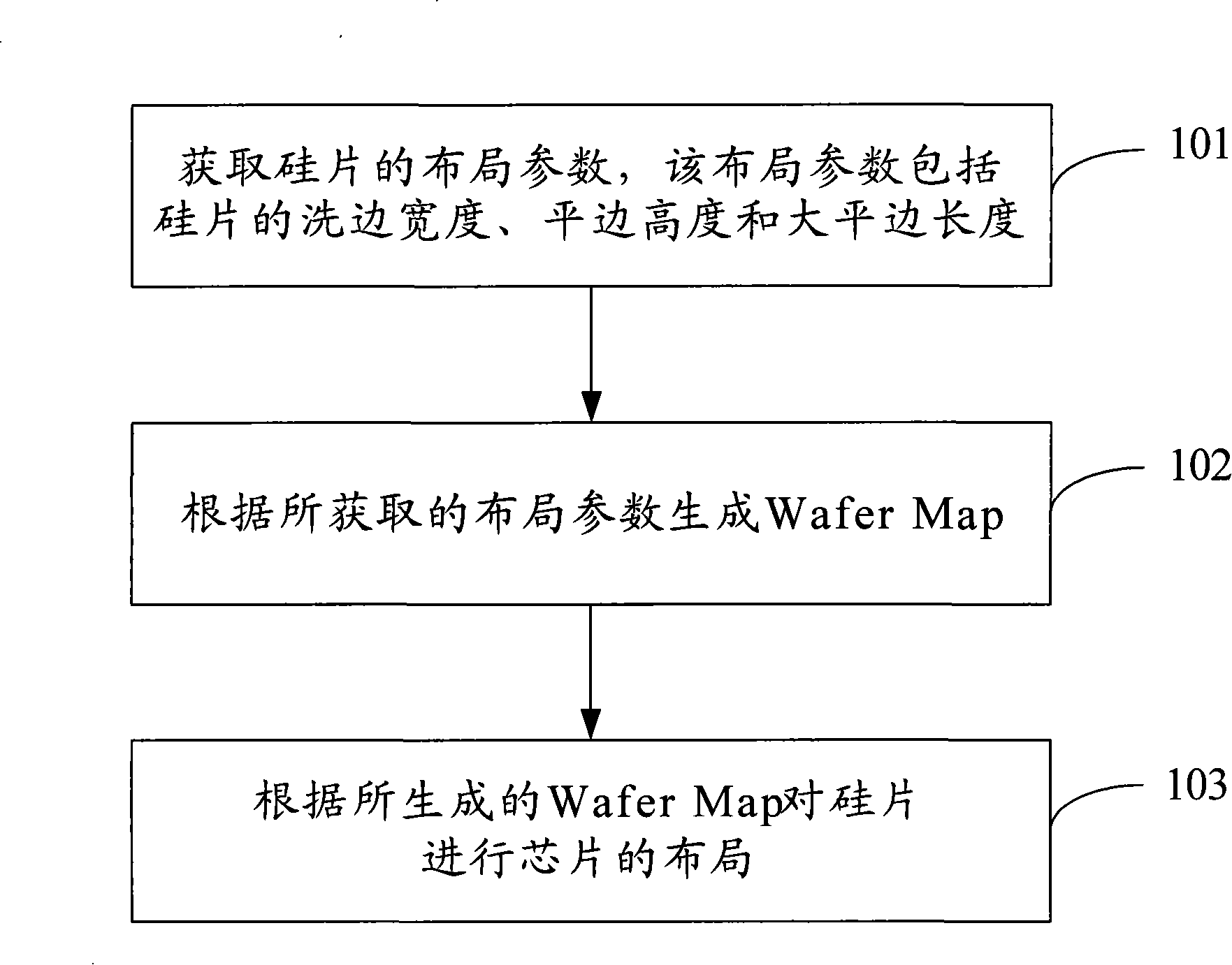
[0027] The technical solutions of the present invention will be further elaborated below in conjunction with the accompanying drawings and specific embodiments.
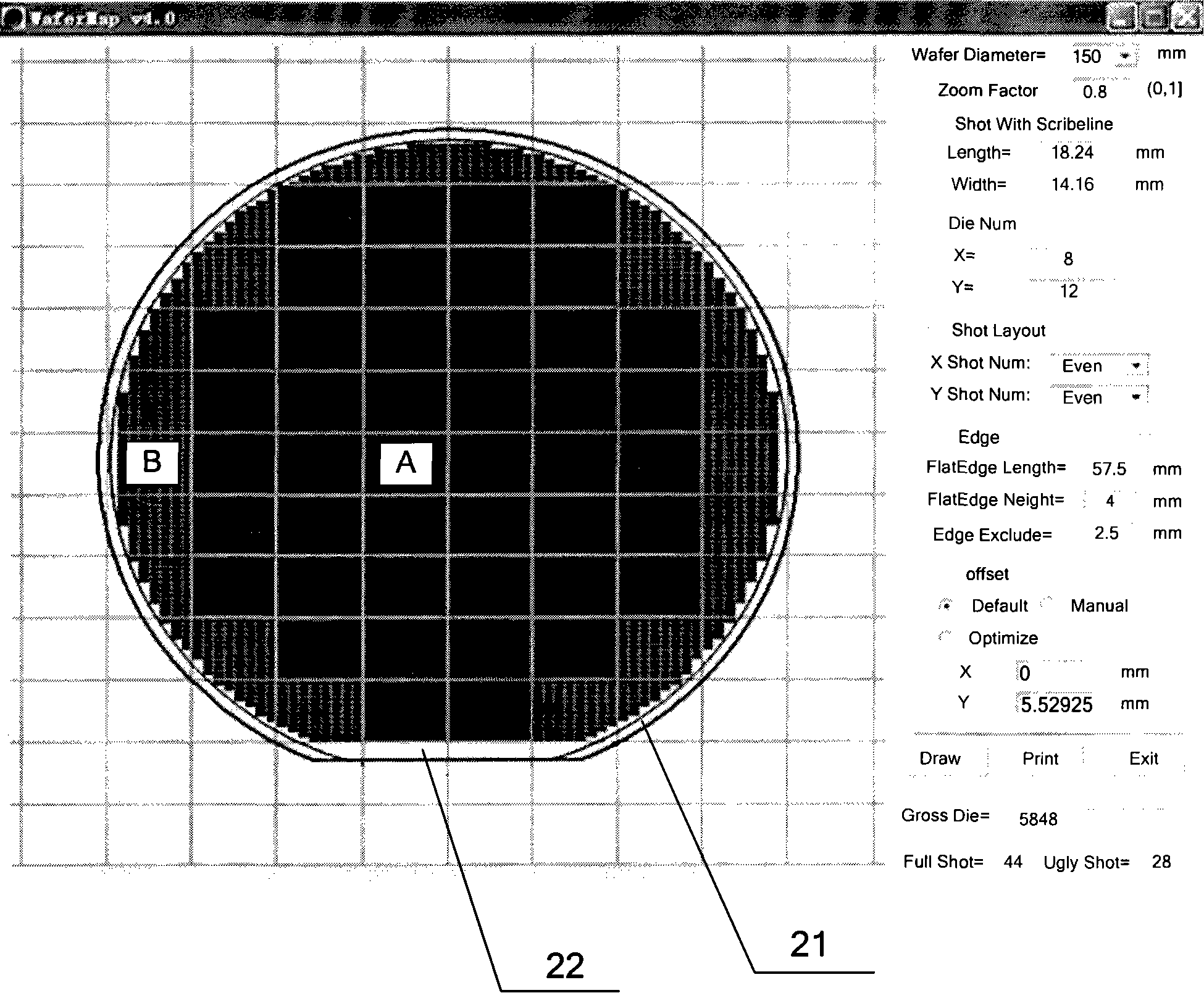
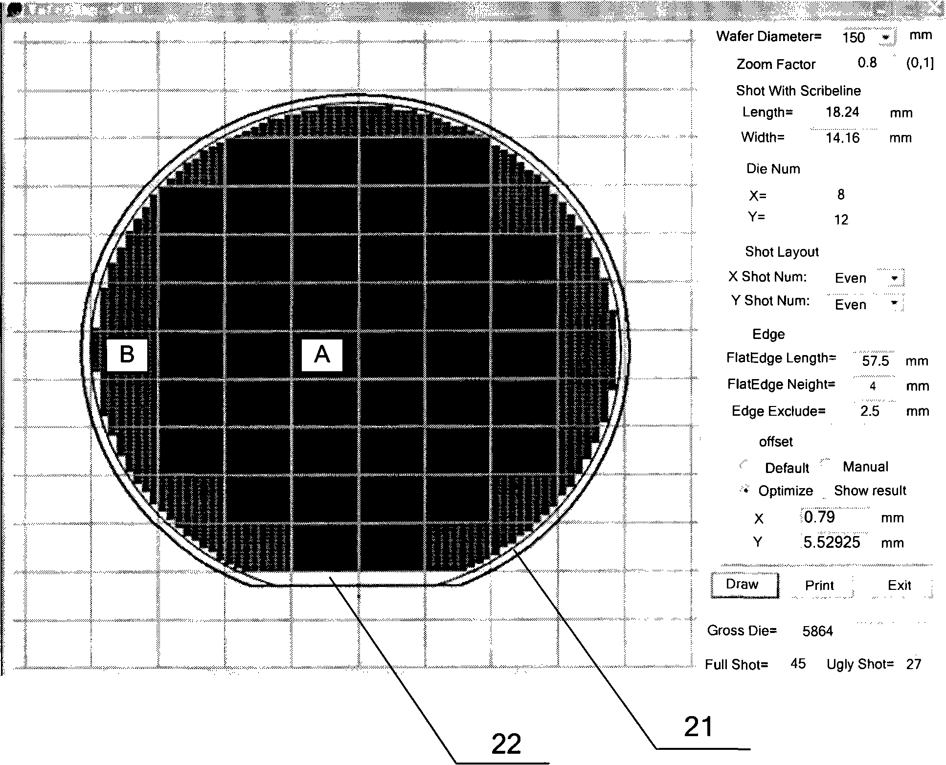
[0028] The present invention provides a method for optimizing chip layout in a silicon chip. According to the actual situation, the layout parameters such as Edge Exclude, FlatEdge Height and FlatEdge Length are set when drawing WaferMap, and the Wafer Map drawn is fine-tuned through the set Offset, which can make the drawing The resulting Wafer Map is closer to the actual silicon wafer, and a more reasonable chip layout in the silicon wafer is obtained.
[0029] A method for optimizing chip layout in a silicon wafer provided by the present invention, such as figure 1 As shown, it mainly includes the following steps:
[0030] Step 101, acquiring layout parameters of the silicon chip, the layout parameters including Edge Exclude, FlatEdge Height and FlatEdge Length of the silicon chip.
[0031] The method for optimi...
PUM
 Abstract
Description
Claims
Application Information