Image processing apparatus and image processing method

An image processing device and image processing technology, applied in image communication, TV, color TV components and other directions, can solve problems such as increased test time and increased cost

Inactive Publication Date: 2008-12-03
CANON KK
View PDF1 Cites 11 Cited by
  • Summary
  • Abstract
  • Description
  • Claims
  • Application Information

AI Technical Summary

Problems solved by technology

Therefore, there are various factors that contribute to the increase in cost, for example, one of the above factors is the increase in test time in the manufacturing process

Method used


Image

  • Image processing apparatus and image processing method
  • Image processing apparatus and image processing method
  • Image processing apparatus and image processing method

Examples


Embodiment Construction

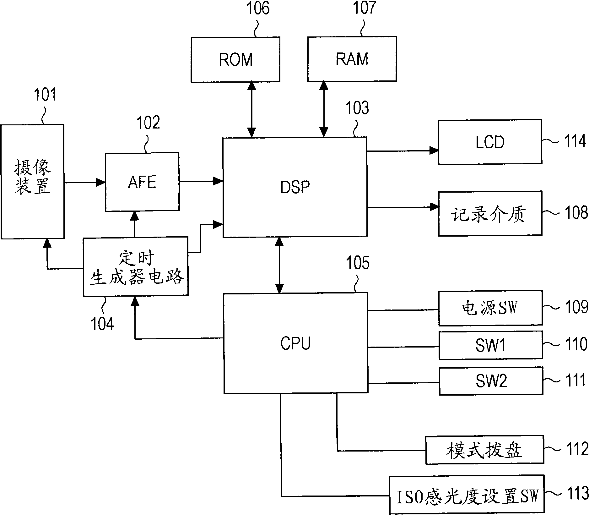
[0037] Exemplary embodiments of the present invention will now be described with reference to the accompanying drawings. figure 1 is a schematic block diagram of the structure of an imaging apparatus as an image processing apparatus according to an embodiment of the present invention.

[0038] The imaging apparatus includes an imaging device 101 , an analog front end (AFE) 102 , a digital signal processor (DSP) 103 , a timing generator circuit 104 , and a central processing unit (CPU) 105 .

[0039] As the imaging device 101 , for example, a CMOS sensor (solid-state imaging device) is used.

[0040] The CMOS sensor includes an amplifier circuit (not shown) capable of switching gain based on ISO sensitivity. All pixel read mode (first operation mode) that reads image data from all pixels, thinning read mode (second operation mode) that reads image data from thinned pixels, and partial clipping read mode Image data including an image captured by the CMOS sensor is read in (the...


PUM


Abstract

The present invention provides an image processing apparatus and image processing method. When pixel data of a solid-state image-pickup device is read in various types of methods to pick up images, a correction process for defective pixels is easily performed at a low cost. As defect-correction data in a case in which a still image is shot, data is used, which is acquired when an image-pickup device is shipped from a manufacturing factory. In a case of an operation in a reading mode for a moving image, immediately before a reading operation is performed, charge is accumulated in a state in which the image-pickup device is shielded from light, and image data is read. Addresses of defective pixels to be corrected are detected from the image data, and stored in a RAM as the defect-correction data. When a moving image is shot, a defect-correction process is performed using the data.

Description

technical field [0001] The present invention relates to a defective pixel correction technique for correcting an image signal associated with a defective pixel that has occurred in a solid-state imaging device. Background technique [0002] In the related art, in solid-state imaging devices such as charge-coupled device (CCD) sensors and complementary metal-oxide-semiconductor (CMOS) sensors, it is known that defective pixels outputting abnormal image signals occur during the manufacturing process of the solid-state imaging devices. It is difficult to completely avoid the occurrence of defective pixels in the manufacturing process of solid-state imaging devices. Therefore, in the related art, a defective pixel correction technique of correcting an image signal output from a defective pixel using image processing has been implemented. [0003] Generally, in the defective pixel correction method used in the related art, the signal output from the defective pixel is corrected ...

Claims


Application Information

Patent Timeline
Patent Type & Authority Applications(China)
IPC IPC(8): H04N5/217H04N3/15H04N5/335H04N5/345H04N5/367H04N5/374
Inventor 木谷一成
Owner CANON KK
Why Eureka
Try Eureka