Current drive circuit and display apparatus

A current-driven, current-driven technology, applied to static indicators, instruments, etc., can solve the problems of reducing the scale of the current driving circuit, increasing the size of the transistor, and difficult to maintain high precision for a long time.

Inactive Publication Date: 2008-12-17
PANASONIC CORP
View PDF1 Cites 9 Cited by
  • Summary
  • Abstract
  • Description
  • Claims
  • Application Information

AI Technical Summary

Problems solved by technology

[0005] However, in the past, the higher the voltage generated in the display panel, the more it was necessary to increase the withstand voltage level of the current drive circuit.
In general, exceeding the withstand voltage level of the transistor will cause the transistor to be extremely unstable in characteristics.
In order to improve this instability, it is necessary to increase the size of the transistor, so it is difficult to reduce the circuit scale of the current drive circuit
In addition, in the manufacturing process of the transistor, it is necessary to add a process for increasing the withstand voltage level, so the manufacturing cost will increase.
[0006] In addition, since the higher the voltage applied to the output terminal of the current drive circuit, the deterioration of the current drive circuit is more likely to occur, so it is difficult to supply the drive current with high accuracy for a long time

Method used


Image

  • Current drive circuit and display apparatus
  • Current drive circuit and display apparatus
  • Current drive circuit and display apparatus

Examples


Embodiment approach 1

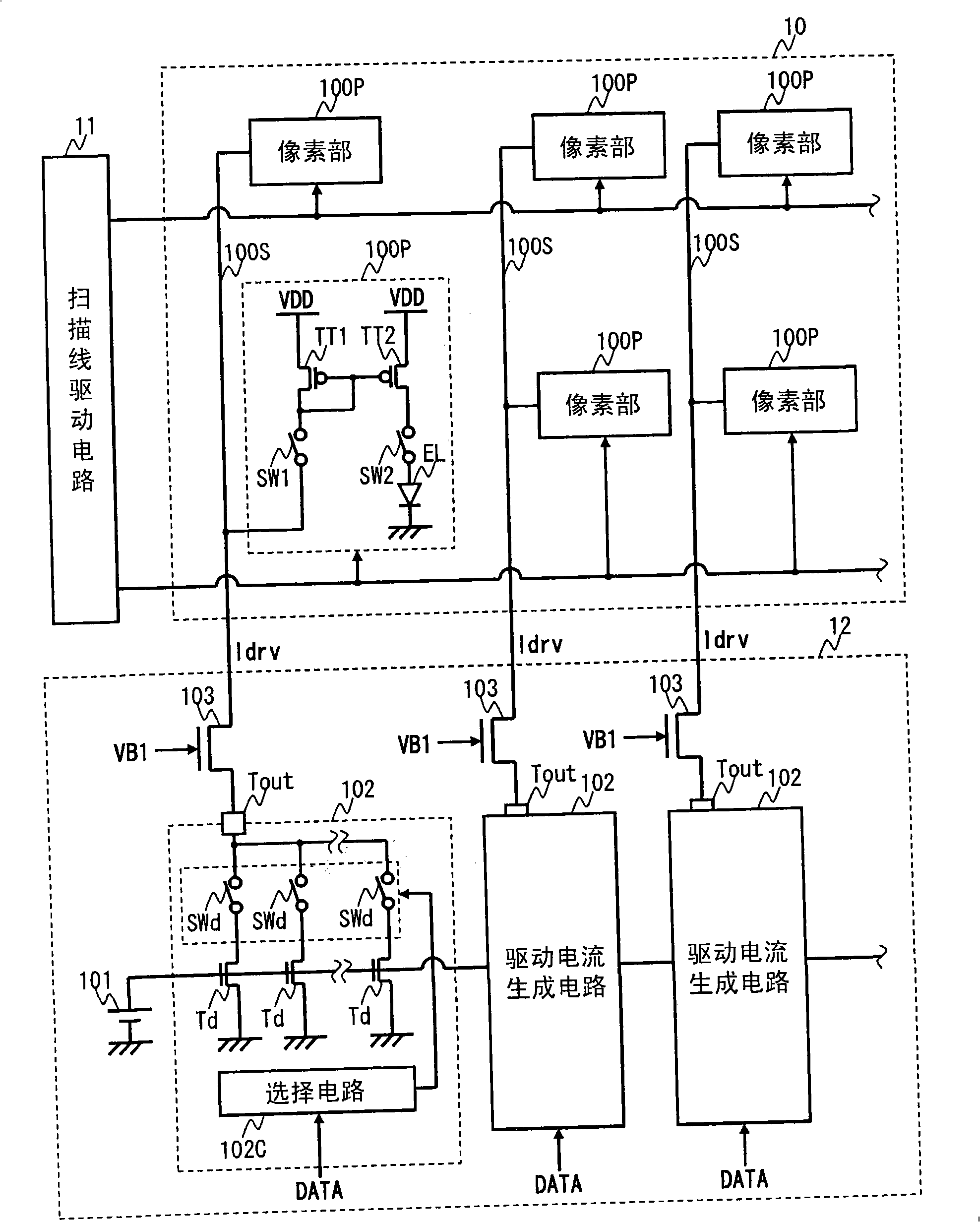
[0031] figure 1 The configuration of the display device in Embodiment 1 of the present invention is shown. This display device includes a current-driven display panel 10 , a scanning line drive circuit 11 , and a current drive circuit 12 .

[0032] "Display panel"

[0033] The display panel 10 includes a plurality of pixel units 100P, 100P, . . . arranged in a matrix, and a plurality of source lines 100S, 100S . The pixel portions 100P, 100P, . . . correspond to one of the source lines 100S, 100S, . . . and include a current-driven light emitting element (here, an organic EL element). In addition, each pixel unit 100P, 100P, ... also has a current duplication mode for duplicating the driving current Idrv supplied to its corresponding source line, and drives its own organic pixel according to the duplicated driving current Idrv. Current drive mode for EL elements.

[0034] For example, the pixel unit 100P includes, in addition to the organic EL element EL, transistors TT1 a...

Embodiment approach 2

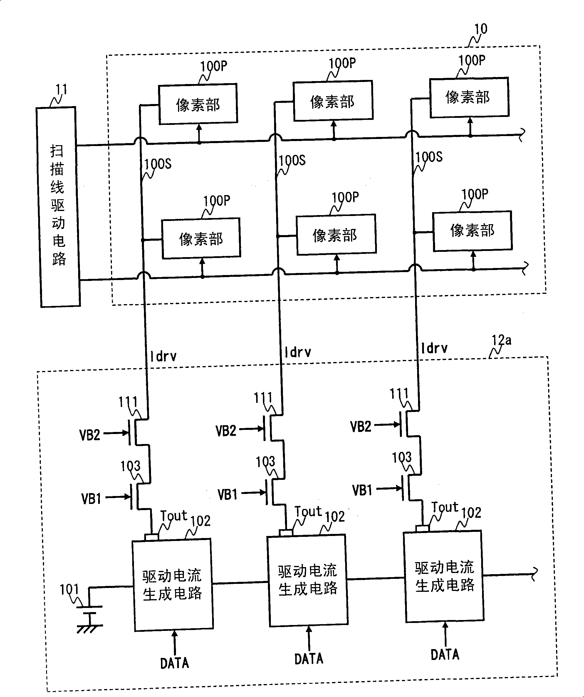
[0051] image 3 The configuration of the display device in Embodiment 2 of the present invention is shown. The display device is in figure 1 In addition to the configuration shown in , a voltage supply circuit 201 and a switch circuit 202 are further provided. In addition, the display device also includes a current drive circuit 22 instead of figure 1 The current drive circuit shown in 12. Other components are balanced figure 1 same.

[0052] "Current Supply Circuit, Switching Circuit"

[0053] The voltage supply circuit 201 supplies an initialization voltage for initializing the voltage of the source lines 100S, 100S, . . . . The switch circuit 202 switches the connection state between the voltage supply circuit 201 and each source line 100S, 100S, . . .

[0054] When the drive current Idrv is supplied to the pixel portion 100P, the drive current Idrv is used to charge and discharge the load capacitance of the drive current generation circuit 102 (the parasitic capacit...

Embodiment approach 3

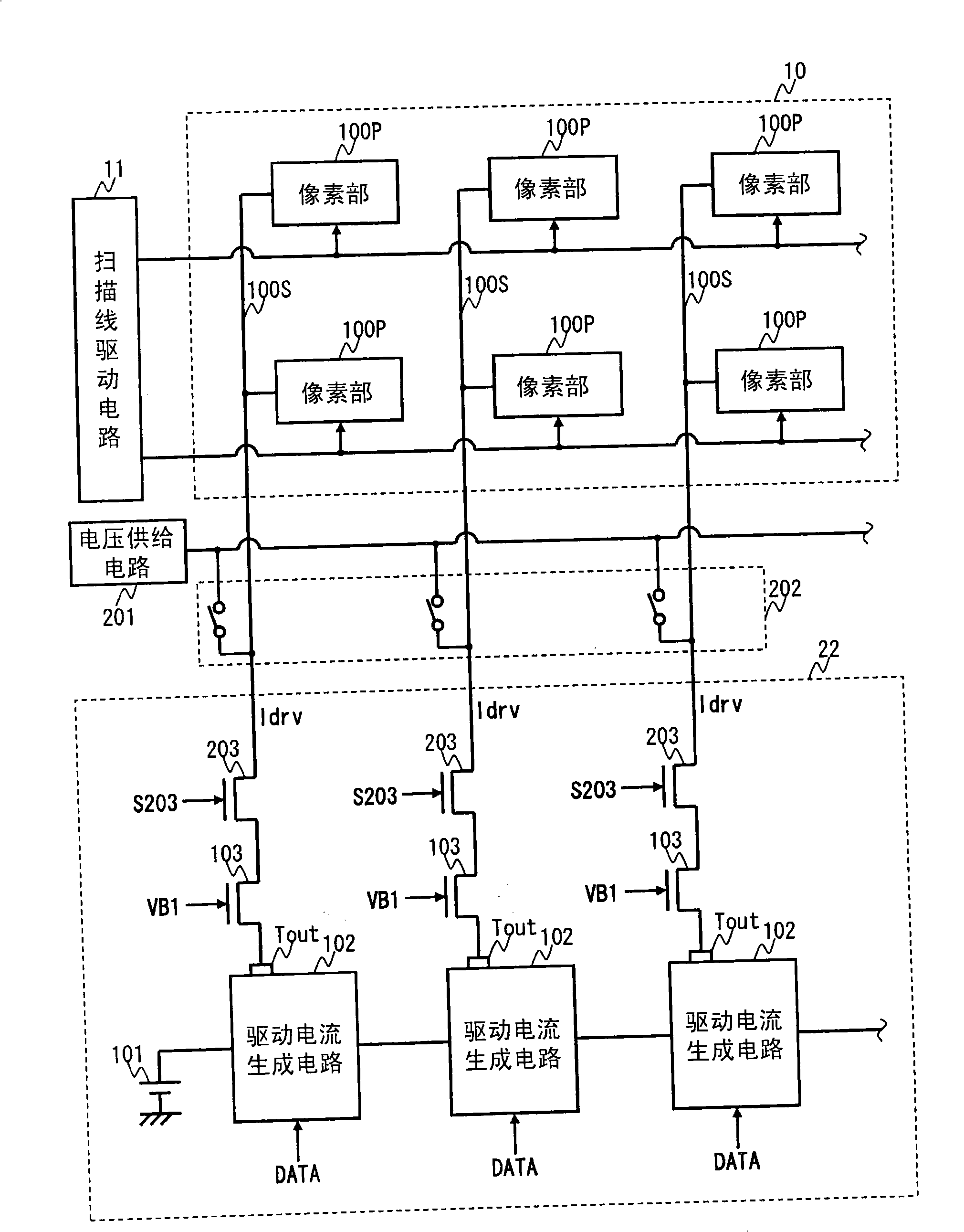
[0066] Figure 6 The configuration of the display device in Embodiment 3 of the present invention is shown. The display device is equipped with a current drive circuit 32 instead of image 3 The current drive circuit 22 shown in . current drive circuit 32, the image 3 In addition to the configuration shown, a compensation transistor 301 is further provided. The other configurations are the same as in 3.

[0067] The compensation transistor 301 has a source and a drain commonly connected to the source of the control transistor 203 , and a gate supplied with a compensation signal S301 for controlling on / off of the compensation transistor 301 . The voltage level of the compensation signal S301 varies inversely to the variation of the control signal S203. For example, when the control signal S203 transitions from low level to high level, the compensation signal S301 transitions from high level to low level.

[0068] The control transistor 203 and the compensation transistor...


PUM


Abstract

A current drive circuit supplies a driving current to a pixel portion included in a current-driven display panel. A driving current generator includes an output terminal for supplying the driving current. A protective transistor has a drain connected to the pixel portion, a source connected to the output terminal, and a gate to which a first bias voltage is supplied. The first bias voltage has a voltage level lower than or equal to a voltage level obtained by adding the threshold voltage of the protective transistor to the breakdown voltage of the driving current generator.

Description

technical field [0001] The present invention relates to a current drive circuit for driving a current drive type drive element of organic EL (Electro Luminescence), and a display device having the same. Background technique [0002] In recent years, development of display devices using current-driven light-emitting elements (for example, organic EL, inorganic EL, etc.) has been actively carried out. This display device includes a display panel including a plurality of pixel units each having a light-emitting element, and a current drive circuit that supplies a drive current corresponding to display data. In this display device, each pixel portion self-replicates the drive current supplied from the current drive circuit, and the light-emitting elements respectively provided in each pixel portion emit light according to the drive current replicated in the pixel portion, thereby displaying an image on the display device. on the display panel. [0003] As disclosed in Internat...

Claims


Application Information

Patent Timeline
Patent Type & Authority Applications(China)
IPC IPC(8): G09G3/30
CPCG09G3/22G09G3/3283G09G2310/0248G09G2330/04
Inventor 小岛宽水木诚小川宗彦西和义大森哲郎
Owner PANASONIC CORP
Why Eureka
Try Eureka