Method for preparing solder pad of printed circuit board
What is AI technical title?
AI technical title is built by PatSnap AI team. It summarizes the technical point description of the patent document.
A technology of printed circuit board and manufacturing method, which is applied in the direction of secondary treatment of printed circuit, coating of non-metallic protective layer, etc., to achieve the effect of simple process, regular graphics and remarkable effect
Click on the blue label to locate the original text in one second.
Reading with bidirectional positioning of images and text.
Examples
Embodiment Construction
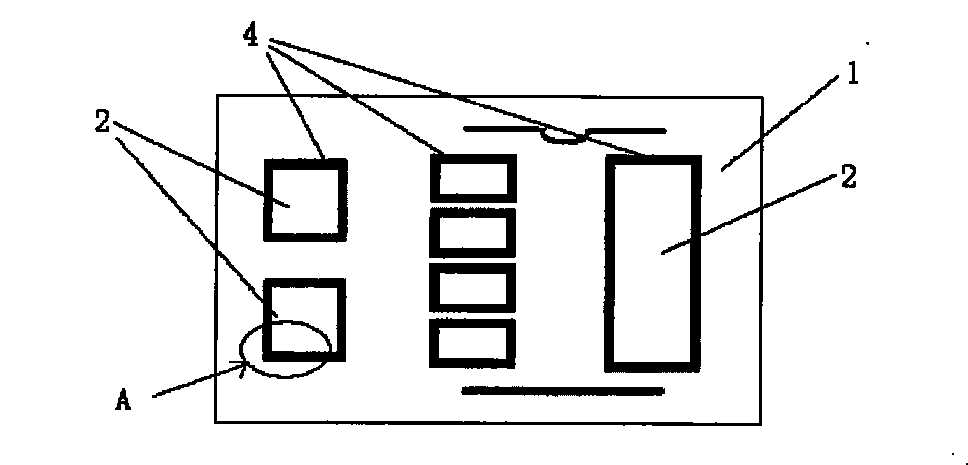
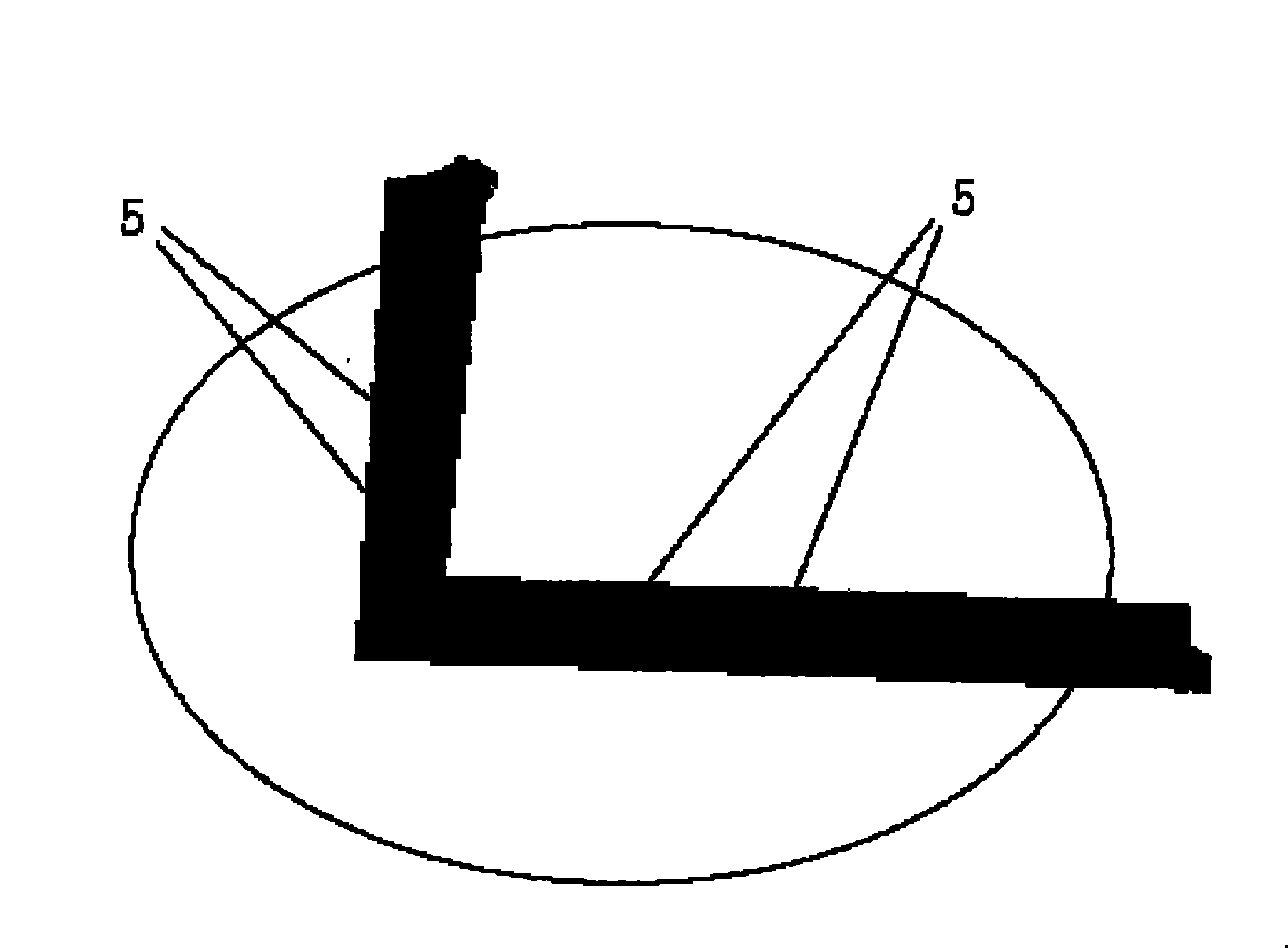
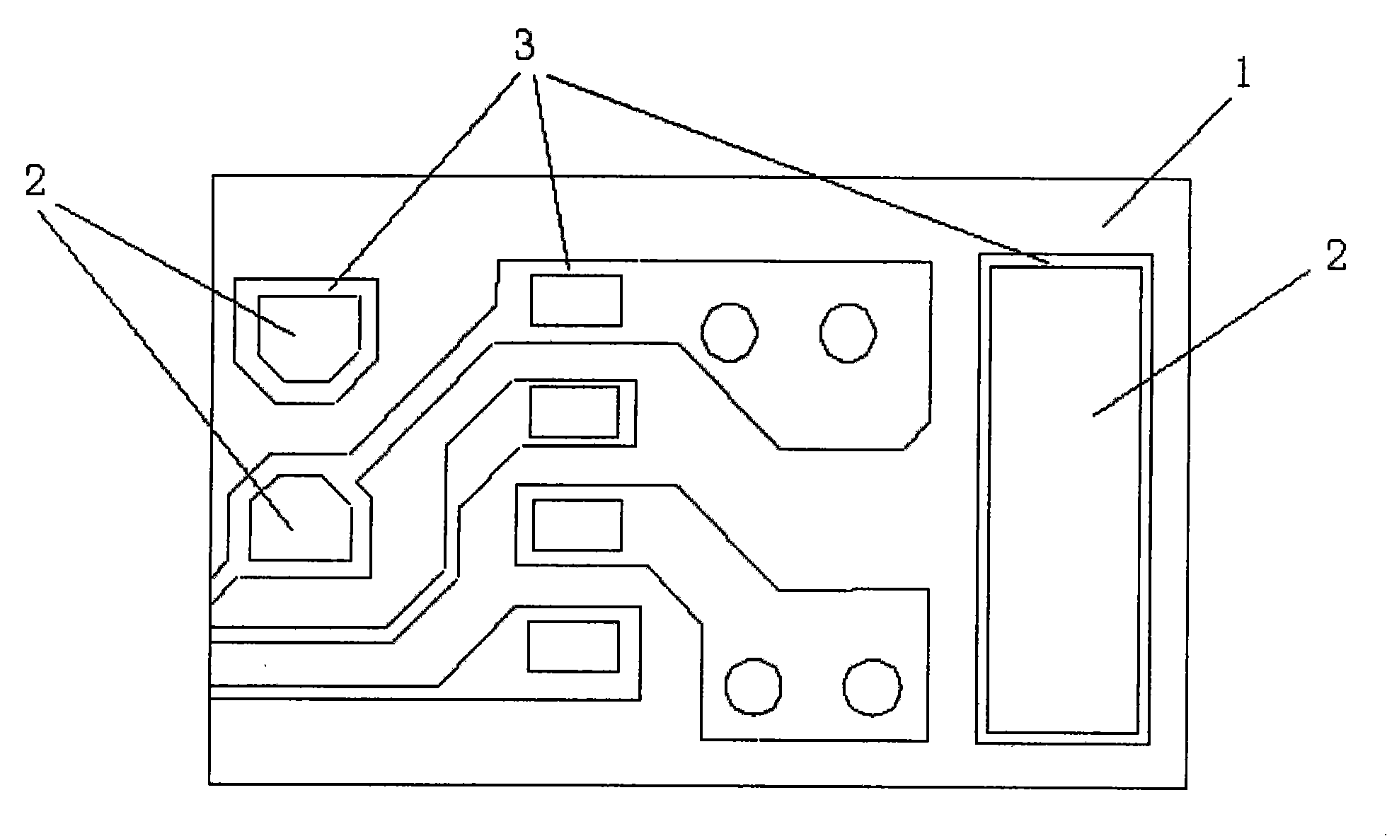
[0018] In the following, a detailed description will be given in combination with the conventional pad forming method and the pad forming method in the present invention to compare the obtained corresponding pad schematic diagrams.
[0019] When making pads in traditional printed circuit boards, the pads and lines are usually formed in one etching process. First, on the printed circuit board substrate with copper on the surface, according to the template of the shape and size of the circuit and pad, the copper layer at the pad and circuit is reserved, and the excess copper is etched away with a chemical solution.
[0020] The copper left after the template pad is etched is the forming pad, and then when the subsequent solder mask process is performed, in order to prevent the solder resist ink from getting on the pad, the solder resist ink needs to be 0.1mm away from the pad.
[0021] The resulting pads such as figure 1 As shown in middle 2, its shape is irregular, and its di...
PUM
Abstract
The invention discloses a method for manufacturing a bonding pad of a printed circuit board. The bonding pad is manufactured and molded in a solder resist sequence when film windowing is exposed. When etching a circuit, the printed circuit board firstly etches out an original bonding pad of which the size is larger than the practically required size of the bonding pad, and concretely the size of each single edge is at least larger for 0.075mm, then the bonding pad with practical size can be obtained after solder resist ink is exposed and developed in the solder resist sequence. A mark point (jointed board MARK for short) which is used for contraposition when the circuit board carries out surface mounting components can be manufactured with the bonding pad in the same sequence so as to guarantee accuracy of relative position of the mark point and the bonding pad and improve precision of surface mounting the piece components. The bonding pad or the jointed board MARK which are obtained by the method of the invention have the advantages of regular shapes and high precision sizes, and the residual copper is left on the periphery of the bonding pad so as to increase bonding pad tensionand be in favor of improving firmness of the piece components.
Description
technical field [0001] The invention discloses a method for manufacturing solder pads in a printed circuit board, in particular to a solder resist forming process for the solder pads of a printed circuit board. Background technique [0002] The existing printed circuit board usually forms the pad and the circuit in the etching process at one time when making the pad, and in the solder resist process, in order to prevent the solder resist ink from getting on the pad, when spraying the solder resist ink, the solder resist ink must be Keep a distance of 0.1mm from the pad. In this way, affected by the precision of the etching process itself, the size tolerance of the pad is relatively large, generally ±20% or ±0.1mm; the solder mask needs to reserve a space of 0.1mm, and there will be a burr of 0.1mm at the connection around the pad. That is, there is a 0.1mm exposed base material that etches the copper layer around the pad; in addition, the copper size of the etched pad is t...
Claims

