Infrared ray transmitting and receiving circuit unit for infrared ray touch screen

A circuit board unit, infrared technology, applied in the direction of electrical digital data processing, input/output process of data processing, instruments, etc., can solve the problem that infrared emission and receiving signals cannot be transmitted to the microprocessor or its corresponding connection, and limit infrared rays Production and sales of touch products, difficulties in high-resolution touch screens, etc., to achieve the effect of improving development and design efficiency, strong consistency, and simple design structure

Inactive Publication Date: 2008-12-24
贺伟
View PDF1 Cites 0 Cited by
  • Summary
  • Abstract
  • Description
  • Claims
  • Application Information

AI Technical Summary

Problems solved by technology

[0002] Since the development of infrared touch technology, it has been relatively mature in technology. From a technical point of view, the principle is very simple, but it is particularly difficult to manufacture high-resolution touch screens of various sizes.
In the existing technology, such as figure 1 , figure 2 In the shown U.S. Patent No. 5,162,783, all control circuits of the infrared touch device, including infrared emitting and receiving tubes, infrared emitting, receiving circuits and microprocessors, are all integrated on the printed circuit board around the outer frame of the touch screen, and are connected through a The RS232 serial port or USB port is connected to the computer. Since the infrared emitting and receiving tubes must be connected to the scanning circuit, if the circuit is cut, the infrared emitting and receiving signals cannot be transmitted to the microprocessor or its corresponding connected circuit. When designing a large-scale infrared touch screen, the existing technology needs to divide the entire transmitting and receiving array into several parts to redesign, increase the number of infrared transmitting and receiving tubes and their control circuits according to the size of the screen, and each independent part needs to be connected to each other , and each independent part needs to be controlled by the microprocessor to complete scanning control and coordinate positioning, and then upload the coordinates of the intercepted object to the computer
Due to the complexity of circuit design in the prior art, when designing each touch screen with different sizes, the circuit basically needs to be changed, and then the printed circuit board required for the product is redesigned and manufactured
Due to the above problems, the production and sales of infrared touch products are largely restricted, and it is even more impossible to make infrared touch products enter the family to reach the level of popularization and application.

Method used


Image

  • Infrared ray transmitting and receiving circuit unit for infrared ray touch screen
  • Infrared ray transmitting and receiving circuit unit for infrared ray touch screen
  • Infrared ray transmitting and receiving circuit unit for infrared ray touch screen

Examples


Embodiment

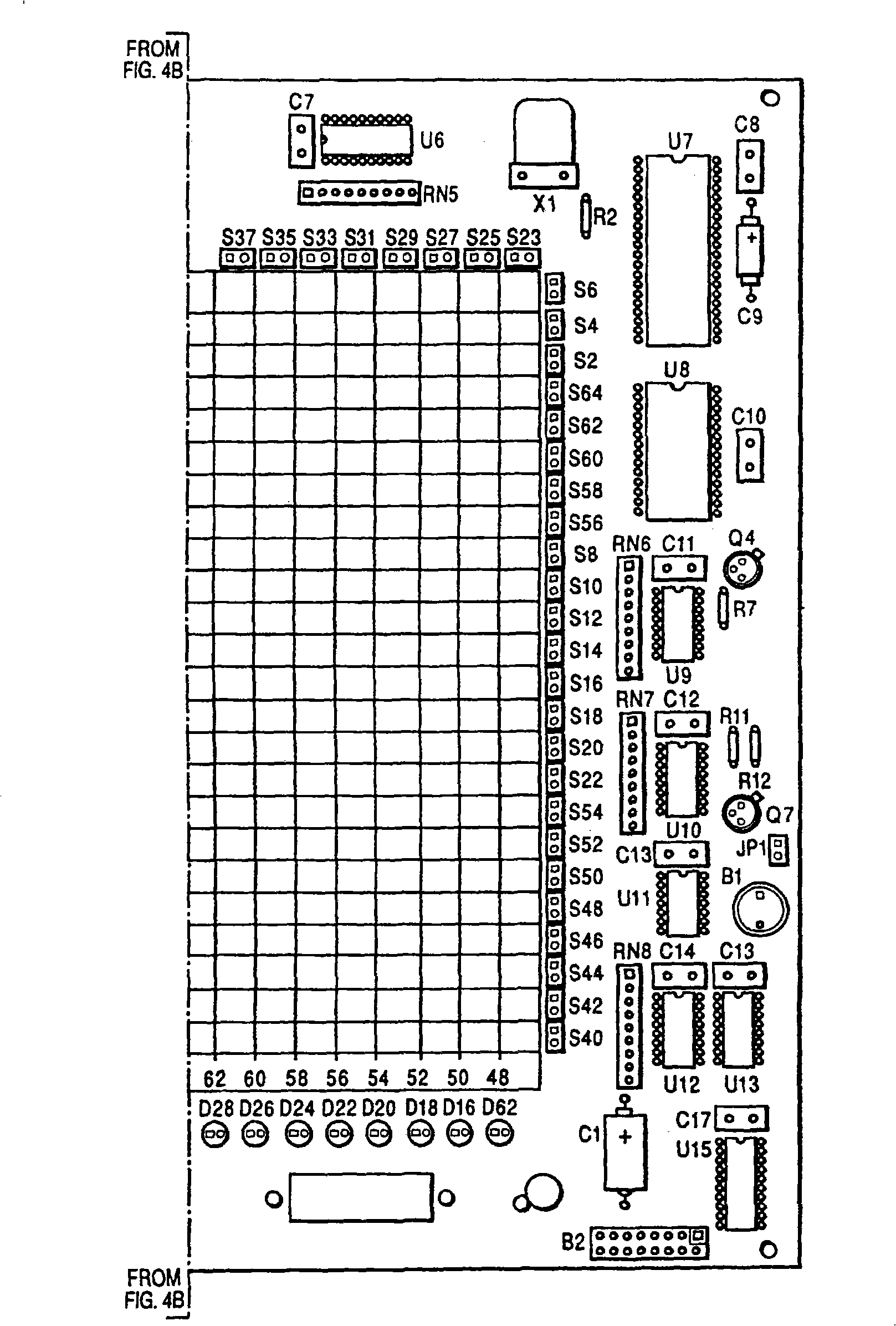
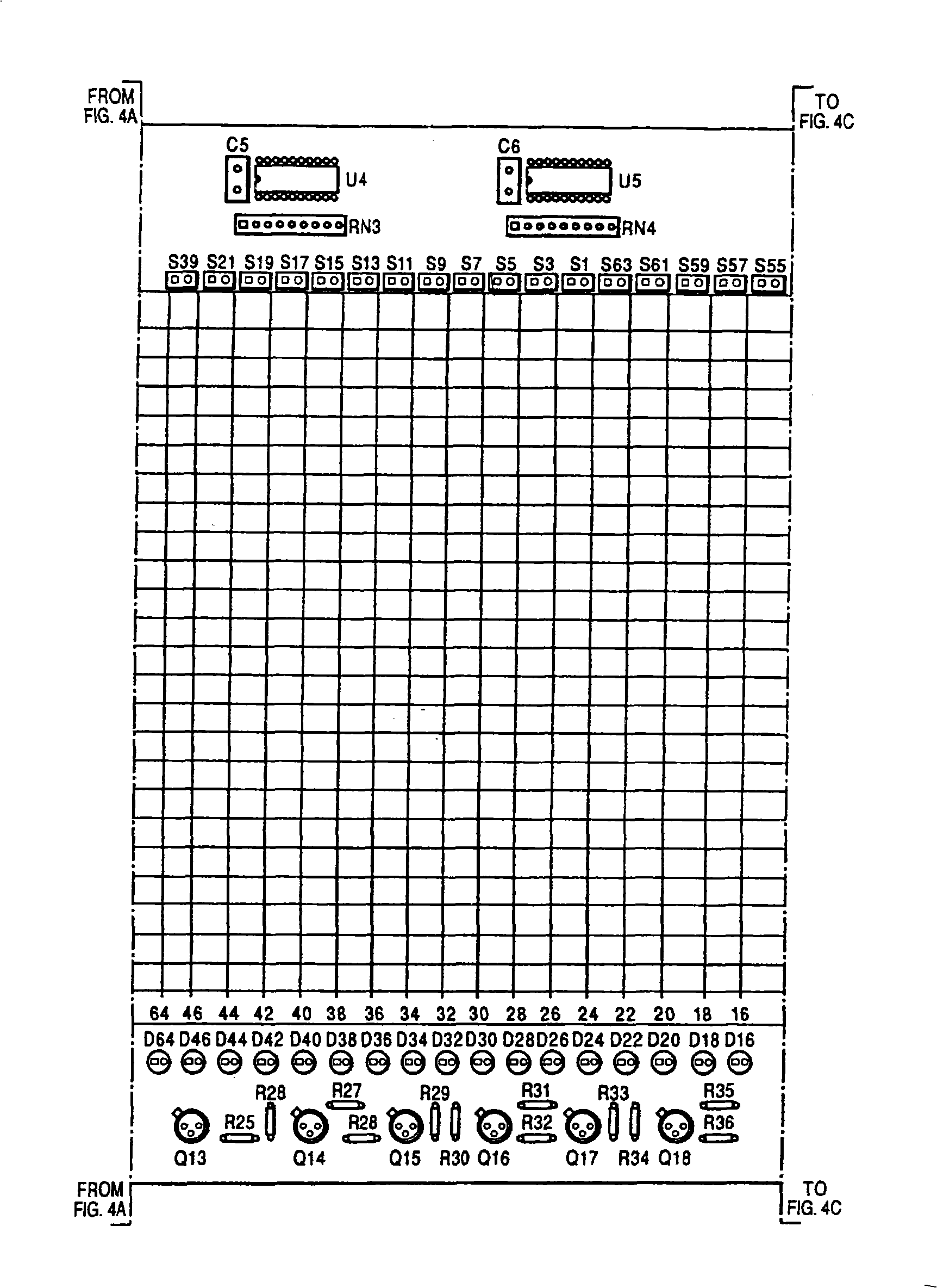
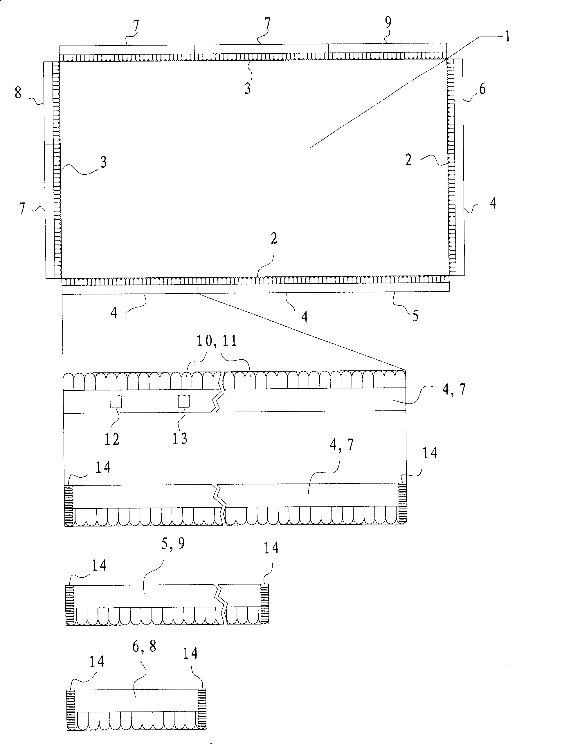
[0021] refer to image 3 , 4, 5 and 6 are an infrared touch screen 1 composed of an infrared emitting and receiving circuit board unit, and a touch screen composed of a standard emitting circuit board unit 4 and cut infrared emitting circuit boards 5 and 6 is arranged around it An infrared emitting array 2; and a receiving array 3 composed of a standard receiving circuit board unit 7 and cut receiving circuit board units 8 and 9 is arranged on the opposite side of the emitting array 2;

[0022] Each transmitting circuit board unit 4, 5, 6 comprises an infrared emitting tube 10 arranged in an array, and is provided with a power supply line 18, a grounding line 19, a clock signal line 16 and an infrared pulse signal line 17 passing through the entire transmitting circuit board unit. One end of the circuit board unit is provided with a row driver 12 and a column driver 13, and the two ends of the circuit board unit are provided with cable welding ports 14 respectively connected t...


PUM


Abstract

The invention discloses an infrared transmitting and receiving circuit board unit which comprises infrared transmitting tubes or receiving tubes arranged in array. The circuit board unit is provided with a power wire, a ground wire and a clock signal wire which run through the whole circuit board unit; one end of the circuit board unit is provided with a column driver and a row driver, wherein, a signal input port of the column driver is connected with the clock signal wire and a signal output port thereof is connected with the signal input port of the row driver; the row drive wires of all infrared transmitting tubes or receiving tubes in the array are connected with the row driver respectively through row control triodes and the column drive wires are respectively connected with the column control wires of the column driver. The infrared transmitting and receiving circuit board unit has simple design and structure, reliable performance, high integration, low production cost and high consistency and reliability during production on a large scale, can be produced on a large scale extensively, greatly improves the efficiency of product development and design, reduces the upfront investment cost of products, increases the speed of the upgrade of products and adds and expands the type of products.

Description

technical field [0001] The invention relates to the technical field of a touch device constructed by infrared emitting and receiving photoelectric devices. Background technique [0002] Since the development of infrared touch technology, it has been relatively mature in technology. From a technical point of view, the principle is very simple, but it is particularly difficult to manufacture high-resolution touch screens of various sizes. In the existing technology, such as figure 1 , figure 2 In the shown U.S. Patent No. 5,162,783, all control circuits of the infrared touch device, including infrared emitting and receiving tubes, infrared emitting, receiving circuits and microprocessors, are all integrated on the printed circuit board around the outer frame of the touch screen, and are connected through a The RS232 serial port or USB port is connected to the computer. Since the infrared emitting and receiving tubes must be connected to the scanning circuit, if the circuit ...

Claims


Application Information

Patent Timeline
IPC IPC(8): G06F3/042
Inventor 贺伟
Owner 贺伟
Why Eureka
Try Eureka