High on-state voltage LED integrated chip with electrostatic protection and manufacturing method thereof

A technology for electrostatic protection and integrated chips, applied in semiconductor/solid-state device manufacturing, circuits, electrical components, etc., can solve the problems of inability to achieve series connection, poor high-voltage resistance, and easy short-circuiting of integrated chips, achieving low cost and occupation. The effect of small area and low manufacturing cost

Inactive Publication Date: 2010-06-09
NANKER GUANGZHOU SEMICON MFG
View PDF0 Cites 0 Cited by
  • Summary
  • Abstract
  • Description
  • Claims
  • Application Information

AI Technical Summary

Problems solved by technology

Since the commonly used LED circuit boards are all aluminum substrates, and the aluminum substrate itself is a conductor, it is very easy to short circuit during the processing of integrated chips and cannot be connected in series.
[0005] Similarly, there are also front-mounted LED integrated chips with electrostatic protection diodes on silicon substrates manufactured by diffusion isolation, which also have the disadvantage of poor high-voltage resistance.

Method used


Image

  • High on-state voltage LED integrated chip with electrostatic protection and manufacturing method thereof
  • High on-state voltage LED integrated chip with electrostatic protection and manufacturing method thereof
  • High on-state voltage LED integrated chip with electrostatic protection and manufacturing method thereof

Examples


Embodiment 1

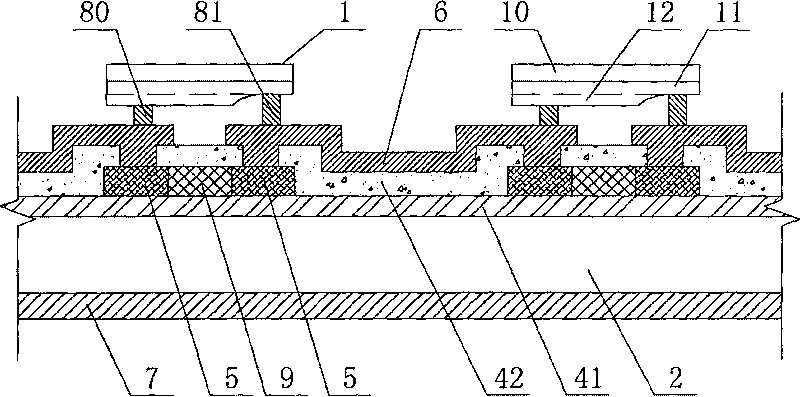
[0058] Such as figure 1 As shown, the high-on-voltage LED integrated chip with electrostatic protection of this embodiment includes several LED bare chips 1 and a silicon substrate 2. The LED bare chips 1 include sapphire (Al 2 O 3 ) A substrate 10 and a gallium nitride (GaN) N-type epitaxial layer 11 and a P-type epitaxial layer 12. Of course, the substrate 10 may also be a substrate made of other materials such as silicon carbide (SiC). The silicon substrate 2 is a P-type silicon substrate. A thermally conductive insulating layer I 41 is formed on the silicon substrate 2. The thermally conductive insulating layer I 41 is composed of a silicon nitride layer. The thermal conductivity of silicon nitride is very high. Generally, the thermal conductive glue is more than 100 times higher. At the same time, the thickness of the thermally conductive insulating layer I 41 is thin, so the thermal conductivity is good, and it can play a good role in heat conduction and heat dissipation. A...

Embodiment 2

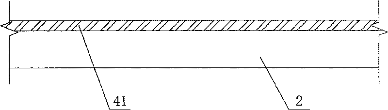
[0072] Such as Picture 11 As shown, the high-on-voltage LED integrated chip with electrostatic protection of this embodiment includes several LED bare chips 1 and a silicon substrate 2. The LED bare chips 1 include sapphire (Al 2 O 3 ) The substrate 10 and the gallium nitride (GaN) N-type epitaxial layer 11 and the P-type epitaxial layer 12. Of course, the substrate 10 may also be a substrate made of other materials such as silicon carbide (SiC). 2 is a P-type silicon substrate. A thermally conductive insulating layer I 41 is formed on the silicon substrate 2. The thermally conductive insulating layer I 41 is composed of silicon dioxide. The thermal conductivity of silicon dioxide is higher, and its thermal conductivity is higher than that of ordinary The thermal conductive glue is several times higher. At the same time, the thickness of the thermally conductive insulating layer I 41 is thin, so the thermal conductivity is good, and it can play a good role in heat conduction and...

Embodiment 3

[0087] Such as Figure 22 As shown, the difference between this embodiment and the first embodiment is that in the high-on-voltage LED integrated chip with electrostatic protection in this embodiment, the LED bare chip 1 is a single-electrode chip, and the LED bare chip 1 includes arsenic. A gallium (GaAs) substrate 10, an N-type epitaxial layer 11, and a P-type epitaxial layer 12. Of course, the substrate 10 may also be a substrate of other materials such as silicon carbide (SiC), and each of the LED bare chips 1 is mounted On each of the metal layers 6 and connected through the metal layers 6 to form a full series circuit, the substrate 10 is bonded to the metal layer 6 with silver paste or tin, and the LED bare chip 1 The electrode contact is welded to the adjacent one of the metal layers 6 by a metal wire 41.

[0088] The remaining features of this embodiment are the same as the first embodiment.


PUM


Abstract

The invention discloses a high continuity voltage LED integrated chip, which has the advantages of static protection, low cost, easy integration, good heat dissipation effect and good high pressure resistant performance and a manufacture method thereof. The chip comprises a plurality of LED bare chips (1) with substrates, N-type epitaxial layers (11) and P-type epitaxial layers (12), a heat conducting insulating layer I (41) and a heat conducting insulating layer II (42) are arranged on a silicon substrate (2) in sequence, a metal layer (6) is arranged on the heat conducting insulating layer II (42), a polysilicon block is respectively arranged in the position of each LED bare chip (1) between the heat conducting insulating layer I (41) and the heat conducting insulating layer II (42), a polysilicon zone I (9) is arranged at the middle part of each polysilicon block, and polysilicon zones II (5) with the polarity being opposite to the polysilicon zone I (9) are arranged on both sides of each polysilicon block, and two separated metal layers(6) are respectively connected with the polysilicon zones II (5) positioned in an identical polysilicon block. The manufacturing method comprises the following steps: forming the two heat conducting insulating layers, forming the polysilicon block, forming the metal layer and flipping the chip.

Description

Technical field [0001] The invention relates to a high conduction voltage LED integrated chip with electrostatic protection; in addition, the present invention also relates to a manufacturing method of the high conduction voltage LED integrated chip with electrostatic protection. Background technique [0002] Flip chip technology is one of the most advanced microelectronic packaging technologies today. It is not only a chip interconnection technology, but also an ideal chip bonding technology. It has raised the circuit assembly density to a new level. Among all surface mount technologies, flip chip can reach the smallest and thinnest package. With the further reduction of the volume of electronic products, the application of flip chip will become more and more extensive. The package in which the LED bare chip is flipped on the substrate is called flip-chip LED. The traditional flip-chip LED uses a larger area and a smaller number of power LEDs, and the cost is relatively high. D...

Claims


Application Information

Patent Timeline
Patent Type & Authority Patents(China)
IPC IPC(8): H01L25/00H01L23/488H01L23/60H01L23/36H01L21/48H01L21/50H01L21/60
CPCH01L24/17H01L2224/16225H01L2224/17H01L2924/1301H01L2924/14H01L2924/00H01L2924/00012
Inventor 吴俊纬
Owner NANKER GUANGZHOU SEMICON MFG
Why Eureka
Try Eureka