Preparing process of gallium nitride based LED large power chip

A gallium nitride-based, preparation technology, which is applied in semiconductor/solid-state device manufacturing, electrical components, circuits, etc., can solve problems that affect the photoelectric performance of gallium nitride materials, reduce the luminous efficiency of chips, and the metal reflective layer is easy to fall off, etc. Achieve the effects of reducing lattice damage, improving contact interface, and reducing light intensity attenuation

Active Publication Date: 2010-08-04
EPILIGHT TECH
View PDF5 Cites 0 Cited by
  • Summary
  • Abstract
  • Description
  • Claims
  • Application Information

AI Technical Summary

Problems solved by technology

[0003] In the existing dry etching N-GaN step process, the mixed gas of chlorine and argon is used as the etching gas, and the chlorine ion is used for chemical reaction etching and the bombardment of argon plasma to remove gallium nitride, which causes The disadvantages are: first, the surface lattice will be destroyed when the plasma bombards the material; second, in the gallium nitride lattice, the atomic weight and binding energy of nitrogen atoms are weaker than those of gallium atoms, so nitrogen atoms are easier to leave the crystal during the bombardment process. grid, resulting in the absence of nitrogen atoms on the surface of gallium nitride after etching, resulting in a non-stoichiometric gallium nitride film on the surface; the third is that the etching products after etching accumulate on the surface of gallium nitride material and are difficult to remove in time In severe cases, the surface of the etched N region will be blackened, which will affect the photoelectric performance of the gallium nitride material, which is not conducive to the diffusion of current on the contact surface and inside the chip, causing local current density to concentrate and generate heat, thereby reducing the temperature of the chip. luminous efficiency
Depositing a metal reflective film on the back of the LED chip after thinning is a common method to improve the heat dissipation and light output rate, but direct evaporation of the metal reflective film will cause the metal reflective layer to fall off easily, the surface will be oxidized and other poor performance

Method used


Image

  • Preparing process of gallium nitride based LED large power chip
  • Preparing process of gallium nitride based LED large power chip
  • Preparing process of gallium nitride based LED large power chip

Examples


Embodiment Construction

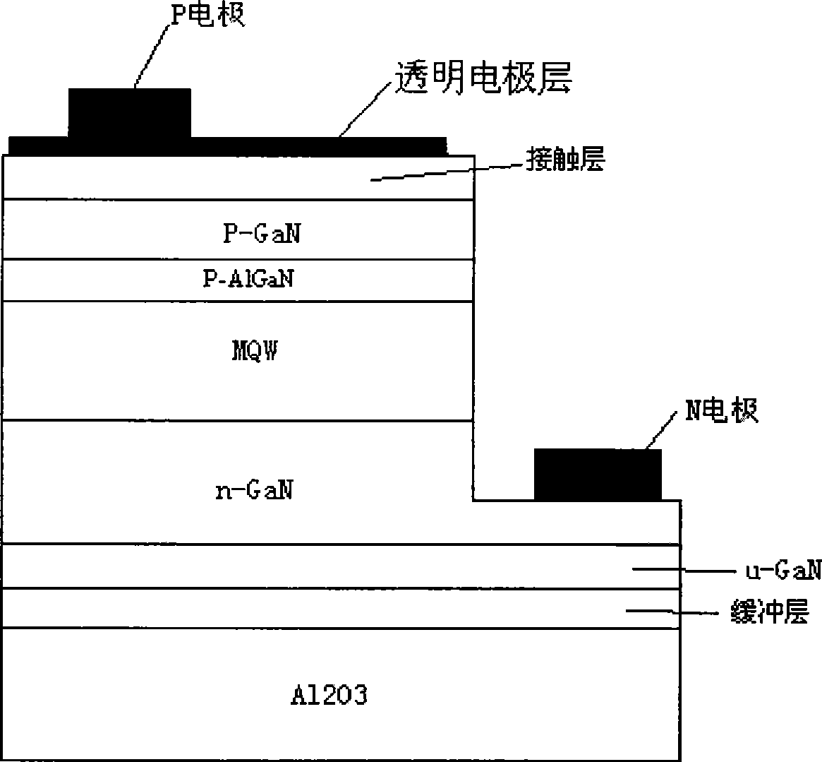
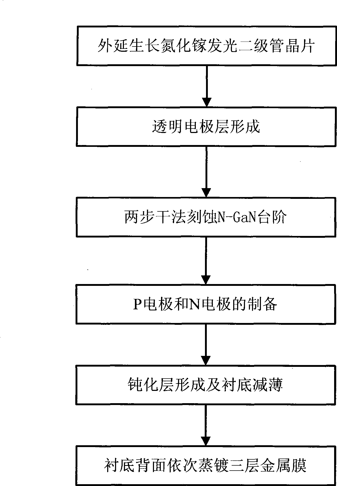
[0011] figure 2 It is the preparation process flow chart of the present invention, wherein the epitaxial growth of gallium nitride light-emitting diode wafer, formation of transparent electrode layer, preparation of P electrode and N electrode, formation of passivation layer and substrate thinning are the same as those of the prior art. The two-step dry etching process of the present invention comprises: the first step, adopts the mixed gas of Cl2 and Ar to carry out main etching, carves N-GaN step; The mixed gas of BCl3 and N2 enters the etching chamber to etch gallium nitride, and etch away the N-GaN layer with a thickness of about 0.05-0.15um. In this embodiment, an inductively coupled plasma reaction etching machine is used for etching. After the gallium nitride wafer is grown and the transparent electrodes are plated, the etching pattern is formed using photoresist and the wafer is sent into the etching chamber for further processing. Two-step etch process. The etching...


PUM


Abstract

The invention discloses a preparation technology of a large-power chip of a GaN-based LED, which adopts two steps of dry etching technology, the first step of which is main etching in which a mixture of Cl2 and Ar is served as an etching gas to etch an N-GaN layer, the second step of which includes that a mixture of BCl3 and N2 is led in and served as the etching gas after finishing the first step to etch away the N-GaN layer which is 0.05um to 0.15um in thickness. The preparation technology of the invention also comprises the following steps of vapor-deposition of three layers of metallic film in sequence on the back of an underlay, namely, a first metallic film with good adhesivity to a sapphire substrate is plated first, then a second metallic film of metallic reflection is plated, andfinally, a third metallic film for protecting metal is vapor-deposited. The light extracting rate of the large-power chip of GaN-based LED prepared by the technology of the invention is increased by about 30 percent and the attenuation of light intensity within 1000 hours is reduced by about 10 percent; furthermore, the cut-in voltage becomes smaller and the chip of the GaN-based LED prepared on the same substrate has better uniformity and stability. The preparation technology of the invention can be applied in the preparation process of the GaN-based LEDs.

Description

technical field [0001] The invention relates to a preparation process of a gallium nitride-based LED chip, in particular to a preparation process of a gallium nitride-based LED high-power chip. Background technique [0002] Gallium nitride-based LEDs are currently the most widely used semiconductor light-emitting diodes. The structure of a common high-power gallium nitride-based light-emitting diode includes (see figure 1 ): Sapphire (Al2O3) substrate, buffer layer, undoped GaN layer, N-GaN layer, InGaN / GaN quantum well active layer (MQW), P-AlGaN layer, P-GaN layer, P-type ohmic contact layer , transparent electrode layer, N electrode and P electrode. The process realization steps are: epitaxial growth of semiconductor light-emitting diode wafer by MOCVD method, including GaN buffer layer to P-type contact layer; deposition of transparent electrode layer by evaporation method, and then performing transparent electrode fusion treatment; dry etching of N-GaN steps; Deposit...

Claims


Application Information

Patent Timeline
Patent Type & Authority Patents(China)
IPC IPC(8): H01L33/00H01L21/306
Inventor 阎占彪黄光辉苏娟梁晖
Owner EPILIGHT TECH
Why Eureka
Try Eureka