Phase change memory cell storage of high reading speed, low operating interference and operating method thereof

A storage unit, reading speed technology, applied in the field of microelectronics

Inactive Publication Date: 2009-01-07
FUDAN UNIV
View PDF0 Cites 13 Cited by
  • Summary
  • Abstract
  • Description
  • Claims
  • Application Information

AI Technical Summary

Problems solved by technology

However, due to the requirement of storing charge, FLASH cannot be expanded unlimitedly with the development of technology generation. It is reported

Method used


Image

  • Phase change memory cell storage of high reading speed, low operating interference and operating method thereof
  • Phase change memory cell storage of high reading speed, low operating interference and operating method thereof
  • Phase change memory cell storage of high reading speed, low operating interference and operating method thereof

Examples


Embodiment Construction

[0022] The invention is described more fully hereinafter in reference to the examples illustrated in the illustrations, providing preferred embodiments but should not be considered limited to the embodiments set forth herein. Rather, these embodiments are provided so that this disclosure will be thorough and complete, and will fully convey the scope of the invention to those skilled in the relevant art.

[0023] Where the referenced figures are schematic illustrations of idealized embodiments of the invention, the illustrated embodiments of the invention should not be construed as limited to the specific shapes of the regions shown in the figures.

[0024] The invention relates to a resistance storage device with high reading speed, high density and low operation interference and a corresponding storage operation method.

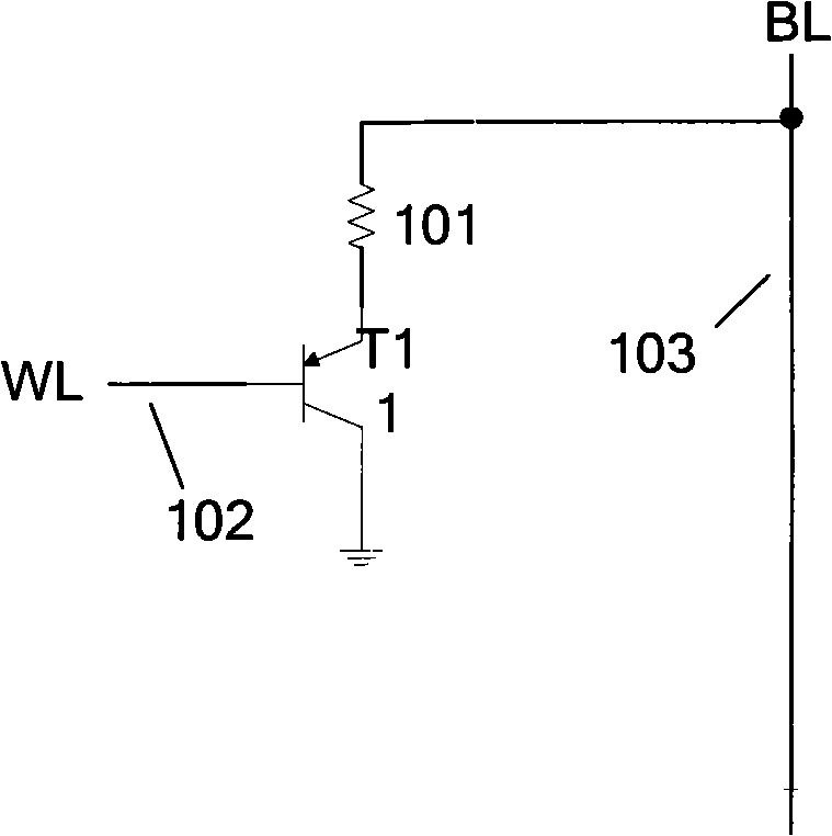
[0025] Figure 1(a) and Figure 1(b) are explained in the technical background of the invention.

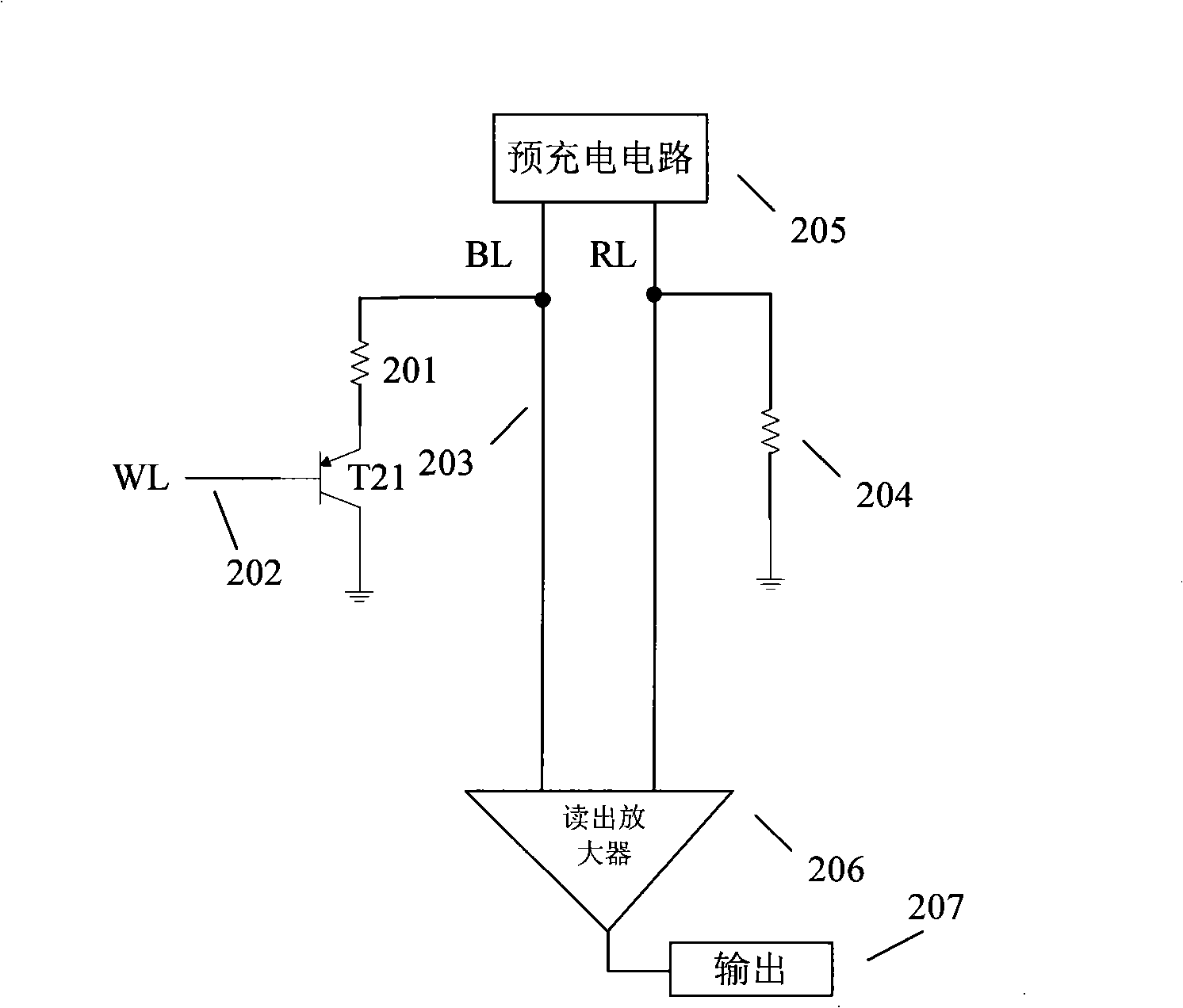
[0026] image 3 The 2B2R memory cell structure proposed by...


PUM


Abstract

The invention belongs to the technical field of microelectronics, and in particular relates to a memory of phase change resistance memory cell structure with high reading speed and low operating interference and a storage operation method thereof; the memory is characterized by comprising a plurality of word lines, a plurality of bit lines and a plurality of memory cells, and each memory cell is positioned at each cross zone between a word line and two bit lines. Each memory cell comprises two phase change memory cells and two gating devices. The two phase change memory cells are connected with different bit lines by the control terminals of respective gate tubes, and share the same word line. The memory and the storage operation method thereof have the advantages of being capable of realizing the application of high reading speed and preventing misreading operation of the selected memory cells in storage operation.

Description

technical field [0001] The invention belongs to the technical field of microelectronics, in particular to a phase-change resistance storage unit structure memory with high reading speed and low operation interference and its storage operation method Background technique [0002] Memory occupies an important position in the semiconductor market. Due to the continuous popularization of portable electronic devices, the share of non-volatile memory in the entire memory market is also increasing, of which more than 90% of the share is occupied by FLASH. However, due to the requirement of storing charges, FLASH cannot be expanded unlimitedly with the development of technology generations. It is reported that the limit of FLASH technology is around 32nm, which forces people to look for the next generation of non-volatile memory with better performance. Recently, resistive switching memory (resistive switching memory) has attracted a lot of attention because of its high density, low...

Claims


Application Information

Patent Timeline
IPC IPC(8): G11C11/56G11C16/02G11C16/10G11C16/26
Inventor 林殷茵徐乐张佶薛晓勇吴雨欣廖启宏胡倍源
Owner FUDAN UNIV
Why Eureka
Try Eureka