Oxide semiconductor, thin film transistor including the same and method of manufacturing a thin film transistor

A technology of oxide semiconductors and thin film transistors, which is applied in semiconductor/solid-state device manufacturing, transistors, semiconductor devices, etc., and can solve the problems of p-SiTFT usage limitations, poor uniformity and large-size substrate manufacturing, and poor cost-effectiveness

Inactive Publication Date: 2009-01-07
SAMSUNG ELECTRONICS CO LTD
View PDF1 Cites 38 Cited by
  • Summary
  • Abstract
  • Description
  • Claims
  • Application Information

AI Technical Summary

Problems solved by technology

Because p-Si TFT is less cost-effective than traditional α-Si TFT, the use of p-Si TFT will be limited
[0007] Since the manufacture of large-sized substrates with a side length greater than 1 m is still not possible due to technical problems (e.g., limitations of production equipment, poor uniformity, etc.), it is difficult to use them in displays (including televisions and computer monitors) and other display products. Using p-Si TFT

Method used


Image

  • Oxide semiconductor, thin film transistor including the same and method of manufacturing a thin film transistor
  • Oxide semiconductor, thin film transistor including the same and method of manufacturing a thin film transistor
  • Oxide semiconductor, thin film transistor including the same and method of manufacturing a thin film transistor

Examples


Embodiment Construction

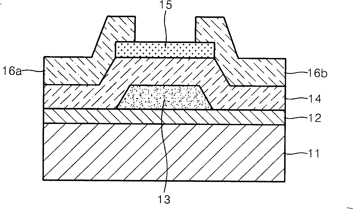
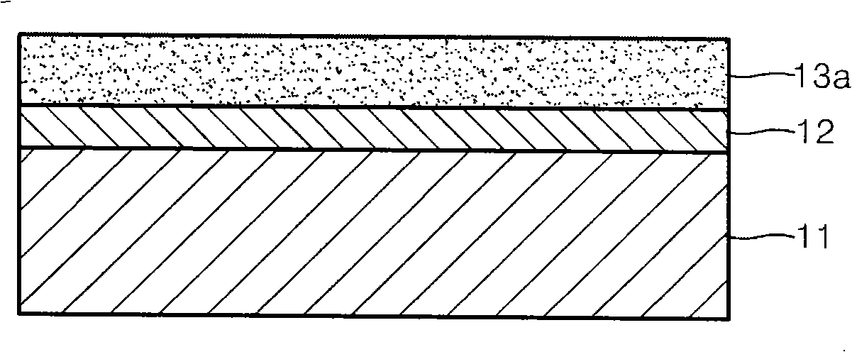
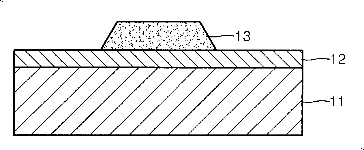
[0032] Reference will now be made in detail to example embodiments, examples of which are illustrated in the accompanying drawings. However, example embodiments are not limited to the embodiments shown below, which are introduced here to provide a simple and complete understanding of the scope and spirit of example embodiments. In the drawings, the thicknesses of layers and regions are exaggerated for clarity.

[0033] It will be understood that when an element or layer is referred to as being "on," "connected to," or "coupled to" another element or layer, the element or layer can be directly on, Directly connected to or bonded to another element or layer, or intervening elements or layers may be present. In contrast, when an element or layer is referred to as being "directly on," "directly connected to" or "directly coupled to" another element or layer, there are no intervening elements or layers present. Like reference numerals refer to like elements throughout. As used h...


PUM

PropertyMeasurementUnit
thicknessaaaaaaaaaa

Abstract

The inventive example relates to a oxide semiconductor containing zinc oxide, thin film transistor containing channel formed by the oxide semiconductor and a method for manufacturing the thin film transistor. The oxide semiconductor comprises: GaInZn oxide, at least one kind of material selected from element of 4B group, oxide of 4B group element, rare earth element and their composition.

Description

technical field [0001] Example embodiments relate to an oxide semiconductor and a thin film transistor including the oxide semiconductor. Other example embodiments relate to an oxide semiconductor including zinc oxide (ZnO), a thin film transistor including a channel formed of the oxide semiconductor, and a method of manufacturing the thin film transistor. Background technique [0002] Thin film transistors can be used in various fields. Thin film transistors can be used as switching devices and driving devices. Thin film transistors can be used as switches to select cross-point memory. [0003] Amorphous silicon thin film transistors (α-Si TFTs) can be used as driving devices and switching devices for displays. α-Si TFT is the most commonly used device for driving devices and switching devices. It is relatively cheap to uniformly form α-Si TFTs on a large-sized substrate with a side length greater than 2 m. As displays become larger and / or sharper, devices with higher ...

Claims


Application Information

Patent Timeline
Patent Type & Authority Applications(China)
IPC IPC(8): H01L29/12H01L29/786H01L21/336
CPCH01L29/7869H01L29/26
Inventor 姜东勋宋利宪朴永洙金昌桢李银河李在喆
Owner SAMSUNG ELECTRONICS CO LTD
Why Eureka
Try Eureka