Method of manufacturing a semiconductor device

A semiconductor and device technology, applied in the field of manufacturing semiconductor devices, to achieve the effect of increasing mechanical stability

Inactive Publication Date: 2009-01-07
NXP BV
View PDF1 Cites 10 Cited by
  • Summary
  • Abstract
  • Description
  • Claims
  • Application Information

AI Technical Summary

Problems solved by technology

Therefore, the method is limited to provide relatively small areas of SOI or SON compared to the entire wafer area

Method used


Image

  • Method of manufacturing a semiconductor device
  • Method of manufacturing a semiconductor device
  • Method of manufacturing a semiconductor device

Examples


Embodiment Construction

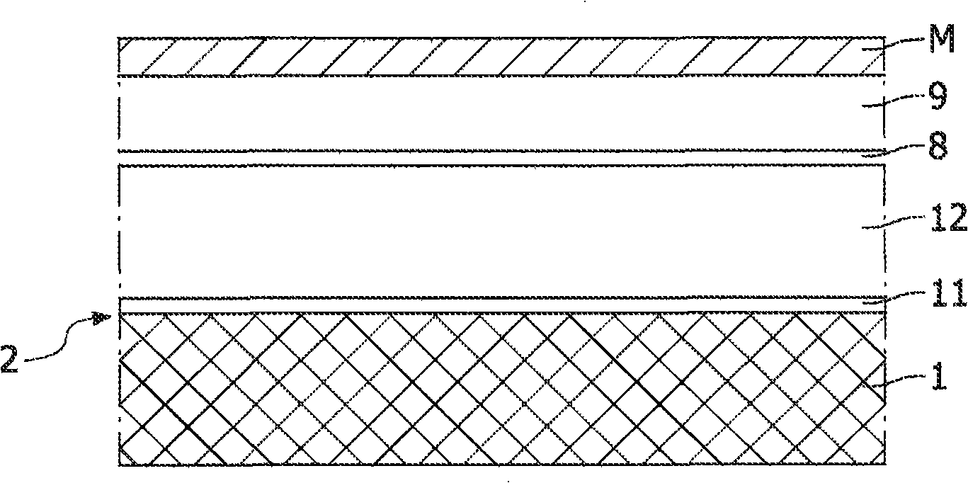
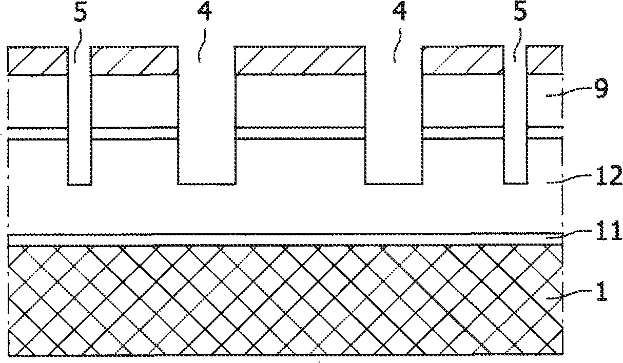
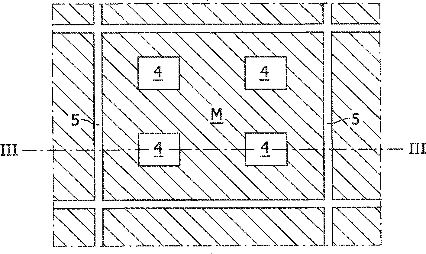
[0037] The first embodiment of the invention shares some of the original process steps of WO-2005 / 093824, so initially reference will be made to Figure 1A , 1B and 1C to describe the first embodiment of the present invention. As used in the method disclosed in WO-2005 / 093824, the method of the present invention uses selective etching to etch the sacrificial layer between the semiconductor film and the bulk substrate. Such as Figure 1A As shown, a layered or stacked structure is formed, and the layered structure includes a substrate 1 , a lower etch stop layer 11 , a sacrificial layer 12 , an upper etch stop layer 8 and a semiconductor layer 9 sequentially from bottom to top. In this example, bulk substrate 1 is a semiconductor substrate of silicon. On this substrate, a SiGe epitaxial layer 11 is grown, with a thickness ranging from 1 to 50 nm, and serving as a lower etch stop layer. The germanium content of this layer 11 is between 10 and 30 at.%. Then, a silicon epitaxi...


PUM


Abstract

A method of manufacturing a semiconductor device is provided, wherein a laminate structure, comprising a sacrificial layer which is sandwiched between two etch stop layers (8,11) and separates a semiconductor membrane (9) from a bulk substrate (1), is used to provide an underetched structure. Access trenches (4) and support trenches (5) are formed in the layered structure through the thickness of the semiconductor layer (9) and through the upper etch stop layer (8). The support trenches extend deeper through the sacrificial layer (12) and the lower etch stop layer and are filled. The sacrificial layer is exposed and etched away selectively to the etch stop layers to form a cavity (30) and realizes a semiconductor membrane which is attached to the bulk substrate via a vertical support structure comprising the filled support trenches.

Description

technical field [0001] The invention relates to a method for manufacturing a semiconductor device, the method comprising: forming a layered structure, the layered structure sequentially includes a substrate, a lower etch stop layer, a sacrificial layer and an upper etch stop layer from bottom to top; first and second sets of trenches through the semiconductor layer and the upper etch stop layer; and through the first set of trenches, etched with an etch selective to the upper etch stop layer and the lower etch stop layer The sacrificial layer is etched to provide a supporting portion of the semiconductor layer over the cavity. In particular, but not exclusively, the invention relates to the transfer of semiconductor thin films from substrates on which they are processed. Background technique [0002] Current semiconductor device technology increasingly requires thin semiconductor bodies on which various types of devices can be processed. This requirement for reduced thickn...

Claims


Application Information

Patent Timeline
Patent Type & Authority Applications(China)
IPC IPC(8): H01L21/762
CPCB81C1/00158B81C2201/014H01L21/76229
Inventor 简·桑斯基韦伯·D·范诺尔特
Owner NXP BV
Why Eureka
Try Eureka