Semiconductor device with field plate and method
A semiconductor and device technology, applied in the field of semiconductor devices with recessed field plates and their fabrication
- Summary
- Abstract
- Description
- Claims
- Application Information
AI Technical Summary
Problems solved by technology
Method used
Image

Examples
Embodiment Construction
[0058] A method of fabricating an NMOS transistor according to an embodiment of the present invention will now be described.
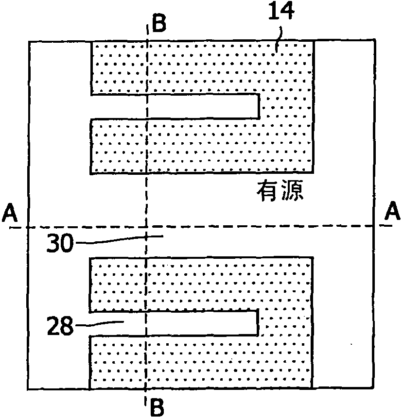
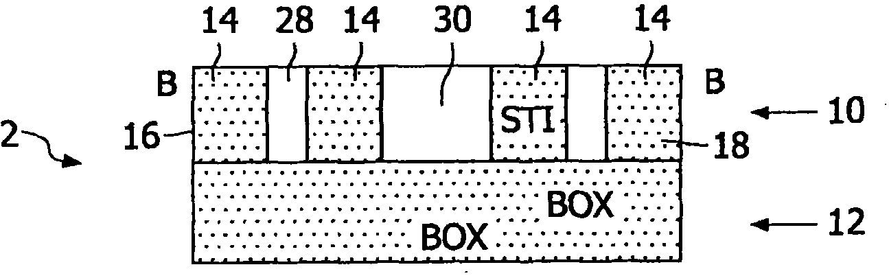
[0059] First, if figure 1 with figure 2 As shown, a silicon-on-insulator (SOI) substrate 2 is provided in which a single crystal silicon device layer 10 is formed on an insulating layer 12 . In this embodiment, the insulating layer is a buried oxide layer, but in alternative embodiments, other silicon-on-insulator technologies, such as silicon-on-sapphire technology, may be used.
[0060] The silicon device layer 10 in an embodiment is 60nm thick.
[0061] Such as figure 1 (top view) and figure 2 As shown in (side view), the first process step is to form a U-shaped insulating region 14 . The U-shaped region is formed using a conventional shallow trench isolation (STI) process in a conventional CMOS process flow, ie shallow trenches 16 are formed and then filled with oxide 18 . The thickness of the silicon device layer 10 is thin enough that t...
PUM
 Abstract
Description
Claims
Application Information
 - R&D
- Intellectual Property
- Life Sciences
- Materials
- Tech Scout
- Unparalleled Data Quality
- Higher Quality Content
- 60% Fewer Hallucinations
Browse by: Latest US Patents, China's latest patents, Technical Efficacy Thesaurus, Application Domain, Technology Topic, Popular Technical Reports.
© 2025 PatSnap. All rights reserved.Legal|Privacy policy|Modern Slavery Act Transparency Statement|Sitemap|About US| Contact US: help@patsnap.com