Detection imaging method and apparatus of strip surface flaw

A strip surface and defect detection technology, which is applied in the direction of optical detection of defects/defects, can solve problems such as poor real-time performance, complex dual-field imaging structure, high cost, and missed detection.

Inactive Publication Date: 2009-01-21
BAOSHAN IRON & STEEL CO LTD
View PDF0 Cites 22 Cited by
  • Summary
  • Abstract
  • Description
  • Claims
  • Application Information

AI Technical Summary

Problems solved by technology

[0004] In view of the above-mentioned shortcomings in the prior art that single-field imaging is prone to missed detection, double-field imaging has a complex structure, high cost, and poor real-time performance, the purpose of the present invention is to provide a method and device for detecting and imaging strip surface defects. The imaging method and device have simple structure, low cost, and good real-time performance, so that the images formed by the same defect on the surface of the strip under different field illumination can be accurately matched

Method used


Image

  • Detection imaging method and apparatus of strip surface flaw
  • Detection imaging method and apparatus of strip surface flaw
  • Detection imaging method and apparatus of strip surface flaw

Examples


Embodiment 1

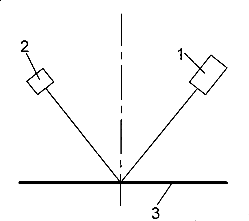
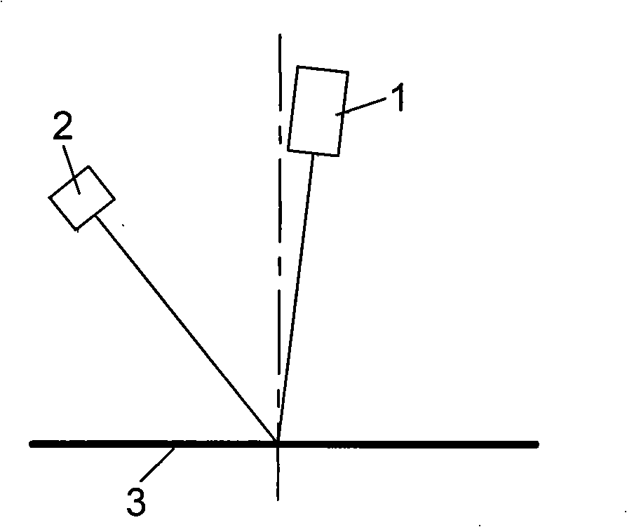
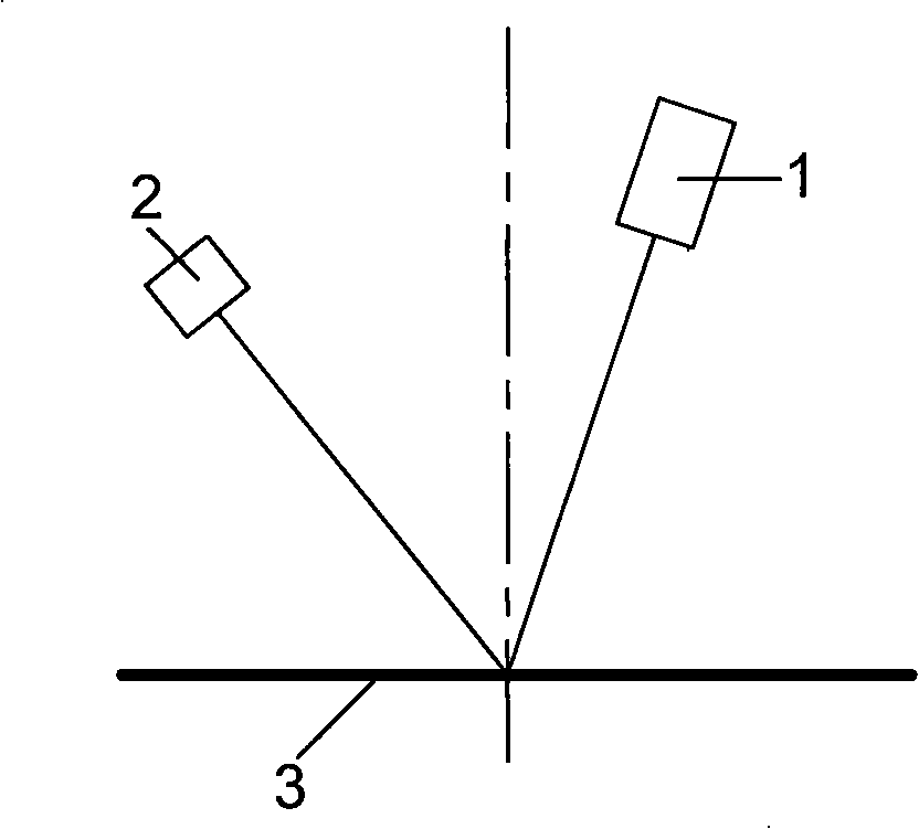
[0037] see Image 6 As shown, the specific steps of the strip surface defect detection and imaging method of the present invention are: first set up a synchronous signal generating unit and generate a synchronous signal, and synchronously control the switching unit and the camera unit; then set up a switching unit, use the switching unit The following two light sources are switched and controlled; then the two light sources are used to alternately illuminate the surface of the strip, and respectively form a single-field imaging with the camera unit, thereby forming the scanning imaging of the strip surface by the camera unit. Among them, the synchronization signal can be directly generated by the synchronization signal generator, or depending on the specific situation, first use the synchronization signal generator to send the original synchronization signal; then use the filter to filter the original synchronization signal; The signal is shaped; finally, the frequency modulat...

Embodiment 2

[0039] see Figure 7As shown, the strip surface defect detection imaging device 10 of the present invention includes a synchronous signal generating unit 11, which is connected to the switching unit 12 and the camera unit 13 respectively, and the synchronous signal generating unit 11 sends a synchronous signal and controls the switching unit 12 and the synchronization of the camera unit 13; the switching unit 12 is connected to two light sources 14a, 14b respectively, and controls the switching of the two light sources 14a, 14b; the two light sources 14a, 14b alternately carry out lighting, and form a single-field imaging with the imaging unit 13, so that the imaging unit 13 can scan and image the strip surface 3. As shown in FIG. 8 , the synchronization signal generating unit 11 is a single synchronization signal generator. When a larger synchronous signal is needed, the synchronous signal generating unit can also be made to include a synchronous signal generator, a filter 1...


PUM


Abstract

The invention discloses an imaging method and a device for detecting band surface defects, wherein the method comprises establishing a sync signal generating unit to generate sync signals, synchronously controlling a switching unit and a camera shooting unit, establishing a light source switching unit, using the switching unit to switch and control the following two light sources, and using the two light sources to alternatively light the surfaces of bands, and respectively and only forming a single ground (a light field, a dark field) to image with the camera shooting unit in a scanning cycle, and obtaining total band surface defect images. The same defect on the band surface can be accurately matched with images which are formed on the same camera shooting unit and different illumination fields. The method avoids the post-treatment problem which is generated by the same defect which repeatedly images, greatly improves the accuracy of detecting the band surface defects, and in addition, and the method further lowers the production cost of the image device and the complexity of the structure.

Description

technical field [0001] The present invention relates to the detection of surface defects on the finished strip, more specifically, to a method and device for detecting and imaging defects on the surface of the strip. All the defects and the images of the same defect on the strip surface under different field illumination can be accurately matched. Background technique [0002] The strip surface defect detection system based on machine vision has been widely used in the world's major strip production enterprises. This type of detection system first uses a CCD camera to obtain the surface image of the strip, and then analyzes the image data to draw a detection conclusion. Therefore, the clarity of the imaging and the difference between the raised defect and the background directly affect the detection effect of the visual inspection system. [0003] There are many commonly used imaging methods at present, including bright field imaging, dark field imaging and transition fiel...

Claims


Application Information

Patent Timeline
Patent Type & Authority Applications(China)
IPC IPC(8): G01N21/88
Inventor 何永辉黄胜标宗德祥王健乔俊良石桂芬陆丽华
Owner BAOSHAN IRON & STEEL CO LTD
Why Eureka
Try Eureka