Silicon based single electron device having double quantum point contact construction and producing method thereof

A single-electron device and contact structure technology, which is applied in the manufacture of semiconductor/solid-state devices, electrical components, semiconductor devices, etc., can solve the problems of uniform control, difficulty in obtaining consistency and stability of the performance of silicon-based single-electron transistors, and achieve overcoming the effects of inconsistency

Inactive Publication Date: 2011-05-04
INST OF SEMICONDUCTORS - CHINESE ACAD OF SCI
View PDF3 Cites 0 Cited by
  • Summary
  • Abstract
  • Description
  • Claims
  • Application Information

AI Technical Summary

Problems solved by technology

The current planar nanofabrication technology is almost difficult to uniformly control the size and even the number of quantum dots of each silicon-based single-electron transistor with this precision, so the performance of the current silicon-based single-electron transistor is almost difficult to obtain good consistency and stability

Method used


Image

  • Silicon based single electron device having double quantum point contact construction and producing method thereof
  • Silicon based single electron device having double quantum point contact construction and producing method thereof
  • Silicon based single electron device having double quantum point contact construction and producing method thereof

Examples


Embodiment Construction

[0049] In order to make the object, technical solution and advantages of the present invention clearer, the present invention will be described in further detail below in conjunction with specific embodiments and with reference to the accompanying drawings.

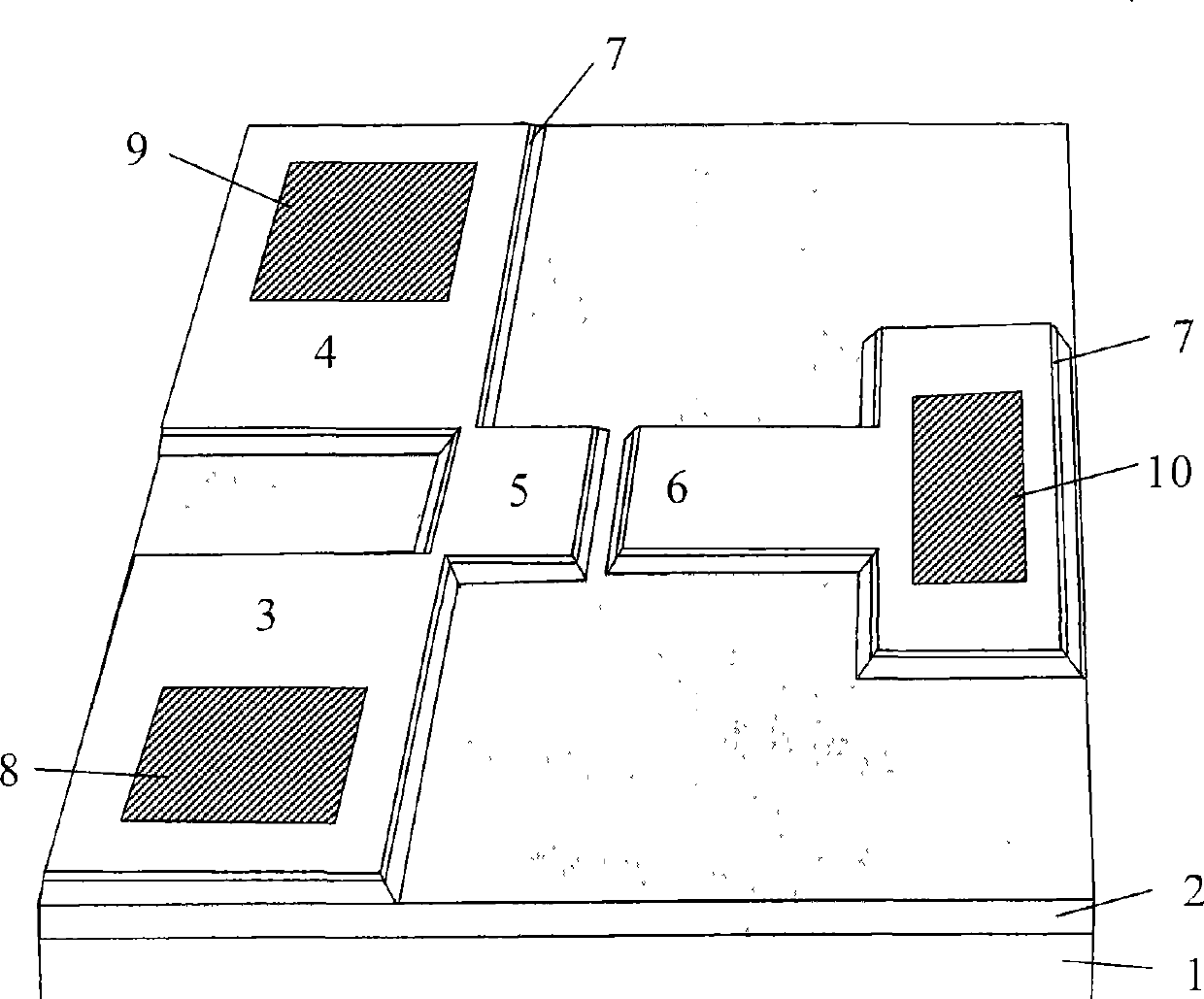
[0050] like figure 1 as shown, figure 1 A schematic structural diagram of a silicon-based single-electron device with a double-quantum point contact structure provided by the present invention, the silicon-based single-electron device includes:

[0051] A silicon-on-insulator SOI substrate for supporting the entire silicon-based single-electron device, including a silicon base 1, an insulating layer 2 and a top layer of silicon;

[0052] Silicon source conductive steps 3, silicon drain conductive steps 4, silicon Coulomb islands 5 and side gate electrode ohmic conductive steps 6 made of top silicon on the SOI substrate, the silicon Coulomb islands 5 are used to store charges, It is located between the silicon source con...


PUM


Abstract

The invention discloses a silicon single electron device with a double-quanta point contact structure. The silicon single electron device comprises a silicon source electrode conduction step, a silicon drain electrode conduction step, a silicon coulomb island, and a side grid electrode ohmic conduction step, which are made on an SOI substrate from silicon on the top layer. The silicon coulomb island is arranged between the silicon source electrode conduction step and the silicon drain electrode conduction step and is connected with the two steps through quanta point contacts, in a shape like the Chinese character pin. The side grid electrode ohmic conduction step at one side of the silicon coulomb island is used to control the charge storage of the silicon coulomb island. The silicon single electron device further comprises a source metal electrode arranged on the silicon source electrode conduction step, a drain metal electrode arranged on the silicon drain electrode conduction step,and a side grid metal electrode arranged on the side grid electrode ohmic conduction step. The invention also discloses a method for fabricating such a silicon single electron device which has a double-quanta point contact structure. The silicon single electron device is capable of steadily controlling single electron transport in batches.

Description

technical field [0001] The invention relates to the technical field of single-electron transport in nanoelectronics, in particular to a silicon-based single-electron device with a double-quantum point contact structure and a manufacturing method thereof. Background technique [0002] Nanoelectronics is one of the important fields of nanotechnology, and it is the continuous development and extension of microelectronics to the microscopic field. At present, the feature size of VLSI has entered the nanoscale (<100nm) range, and the impact of quantum effects has become more and more prominent in the process of scaling down CMOS devices. The nano-solid structure produced by single atomic layer thin film epitaxial growth technology, tunnel probe technology and advanced photolithography technology shows peculiar quantum effects. On the basis of these effects, people have invented resonant tunneling devices and single-electron devices. , quantum dot devices and other new quantum...

Claims


Application Information

Patent Timeline
Patent Type & Authority Patents(China)
IPC IPC(8): H01L29/772H01L21/335
Inventor 韩伟华杨香
Owner INST OF SEMICONDUCTORS - CHINESE ACAD OF SCI
Why Eureka
Try Eureka