


Quick Research
Generate reliable direction feasibility study reports for your R&D in just a few steps.

Technical Q&A
Discover and master advanced knowledge NOW. Basics, ideas, possibilities, all at once.

Find Solutions
As an expert in R&D theories, this can generate solutions to your technical problems instantly.

Evaluate Feasibility
Analyze your overall solution with one click, know your potential R&D risks in advance.

Monitor Landscape
Get weekly tech updates, stay abreast of the latest tech innovations and key insights.
Multiple die integrated circuit package
A technology of die and package, which is applied in the field of semiconductor device assembly and packaging, and can solve the problems of low cost, daily use and non-customized IC chips, etc.
- Summary
- Abstract
- Description
- Claims
- Application Information
AI Technical Summary
Problems solved by technology
Method used
Image

Examples
Embodiment Construction
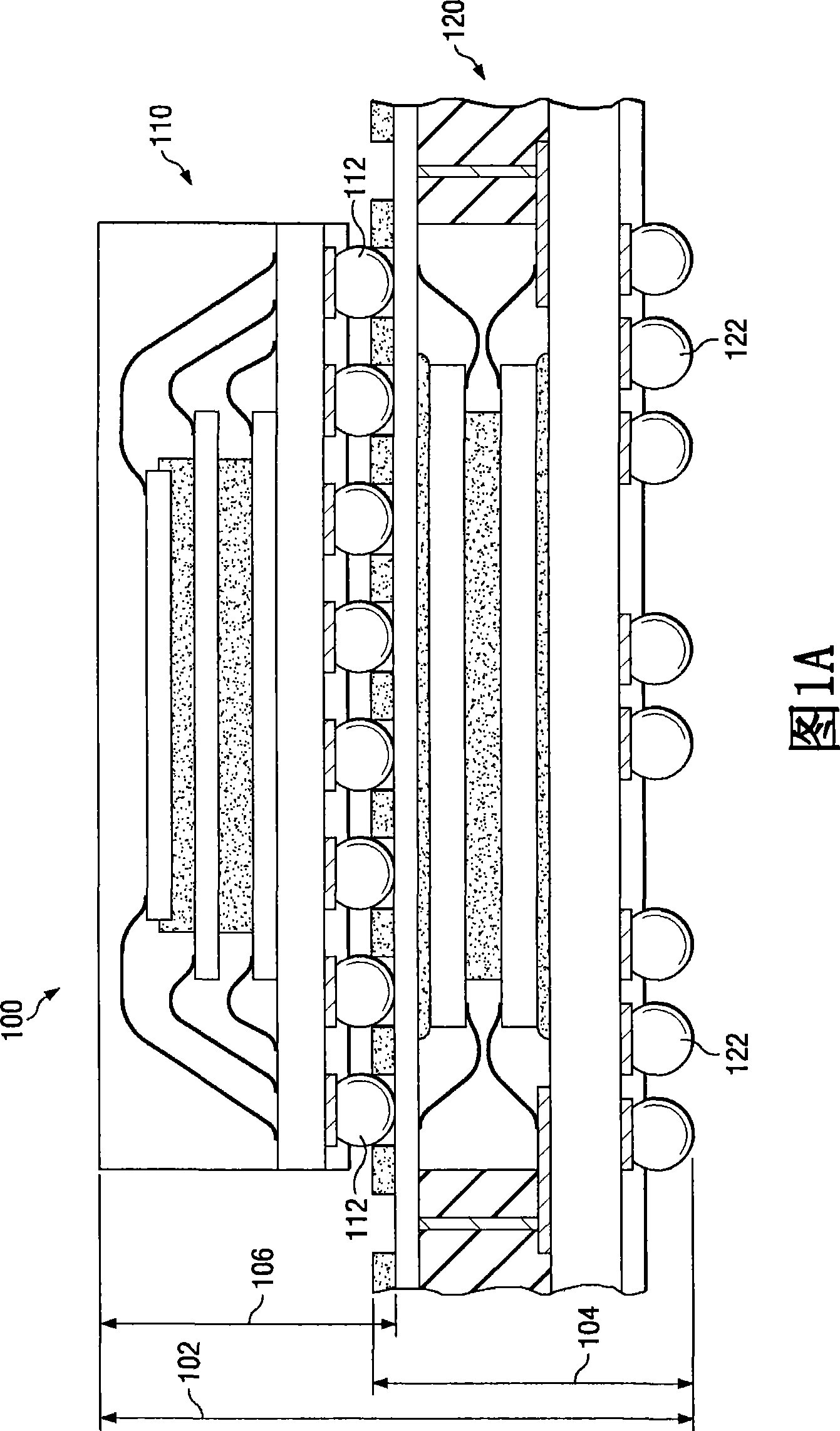
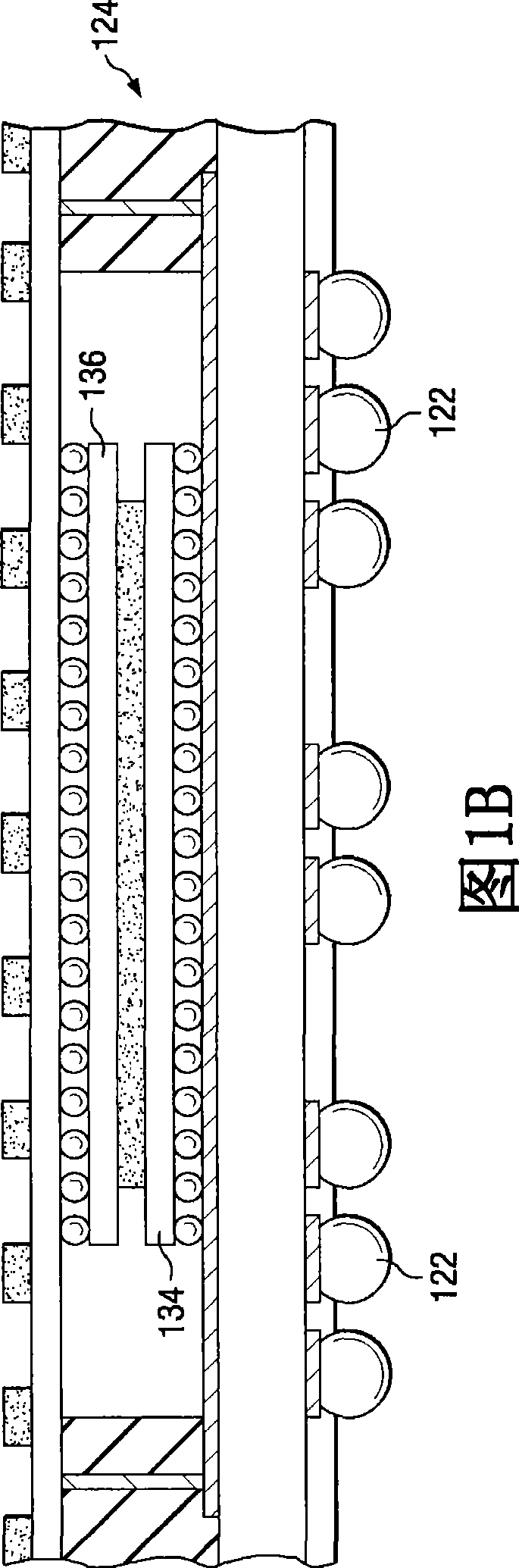
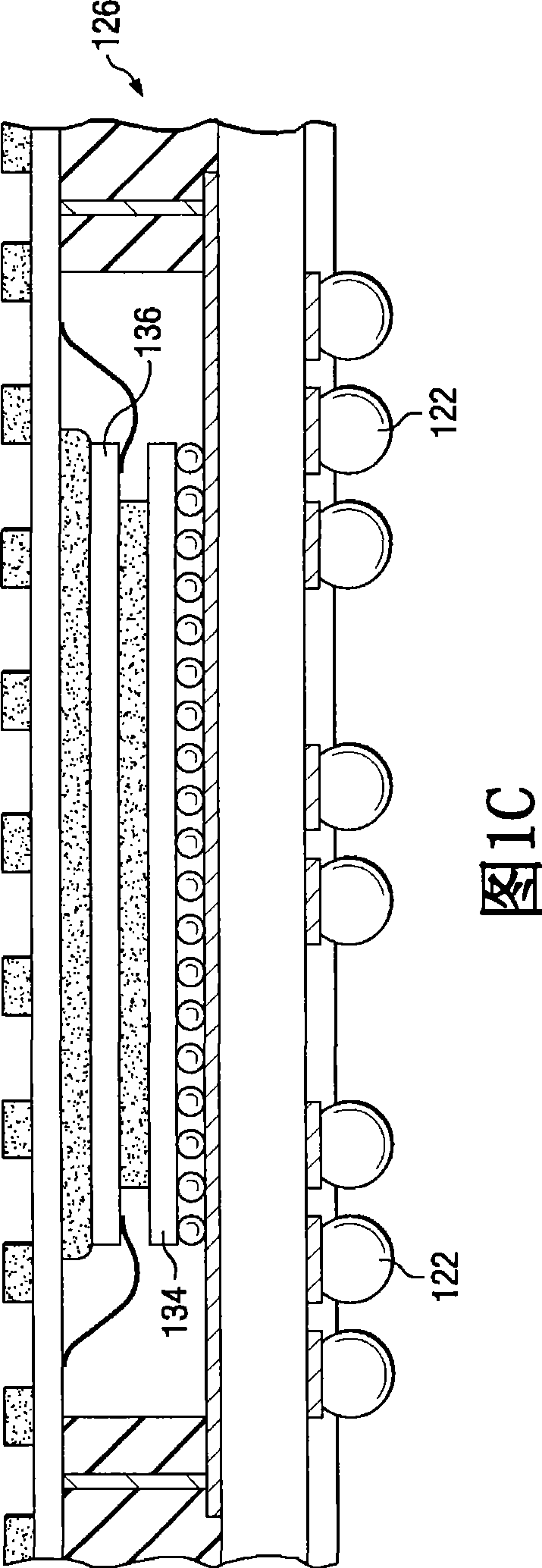
[0012] [0009] Traditional tools and methods for manufacturing semiconductor devices with a PoP structure are limited by the constraints of the top package, the bottom package and their interfaces. These constraints can include a bottom package that is limited to one die, limited input / output (I / O) connections due to the perimeter matrix coverage area of the top package, and customized (non-daily) more The use of expensive memory chips as top packages. This problem can be solved by using improved systems and methods for manufacturing semiconductor devices with PoP structures. According to one embodiment, in an improved system and method for manufacturing a semiconductor device having a PoP structure, a bottom layered substrate (BLS) is formed to include an interconnect pattern (IP) coupled to a plurality of conductive bumps (PCB) . The top substrate (TS) is formed by forming a polyimide tape (PT) pasted on the metal layer (ML) and a top die connected to the opposite side of the M...
PUM
| Property | Measurement | Unit |
|---|---|---|
| Thickness | aaaaa | aaaaa |
| Height | aaaaa | aaaaa |
Abstract
Description
Claims
Application Information
 - R&D Engineer
- R&D Manager
- IP Professional
- Industry Leading Data Capabilities
- Powerful AI technology
- Patent DNA Extraction
Browse by: Latest US Patents, China's latest patents, Technical Efficacy Thesaurus, Application Domain, Technology Topic, Popular Technical Reports.
© 2024 PatSnap. All rights reserved.Legal|Privacy policy|Modern Slavery Act Transparency Statement|Sitemap|About US| Contact US: help@patsnap.com