Composite blooming
An optical film and microstructure technology, applied in the field of composite optical film, can solve the problems of high price, complex backlight module, and increased thickness of backlight module
- Summary
- Abstract
- Description
- Claims
- Application Information
AI Technical Summary
Problems solved by technology
Method used
Image
Examples
Embodiment 1
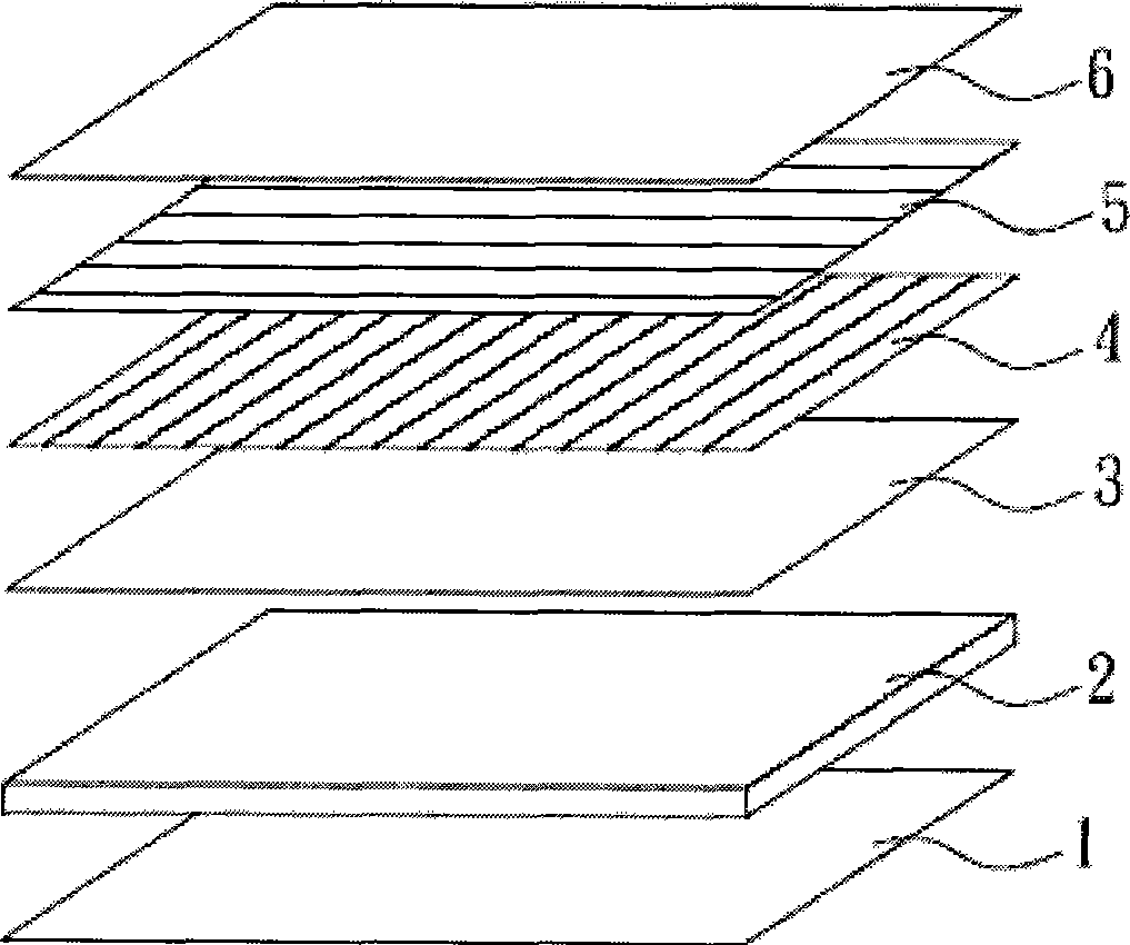
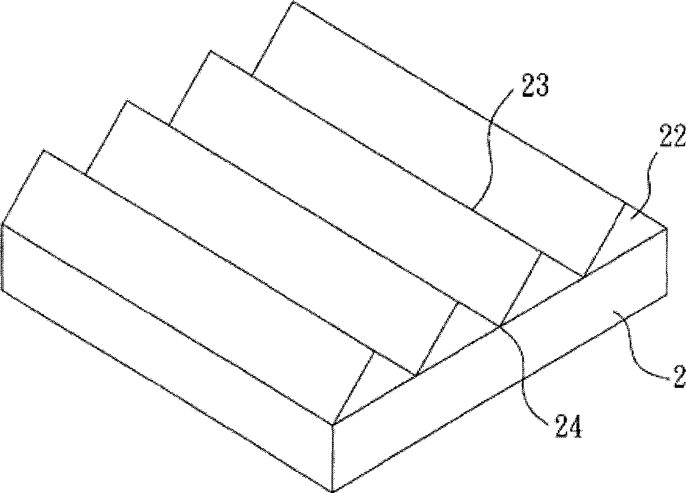
[0074] On the surface of the substrate with a diffuse microstructure with a haze of 50% in Table 1, coat an acrylic resin coating with a thickness of about 15 μm, and form a prism pattern on the coating by roller embossing, and then reuse The composite optical film of the present invention is obtained by hardening it with high-energy ultraviolet rays (UV).
Embodiment 2
[0076] On the surface of the substrate with a diffuse microstructure with a haze of 90% in Table 1, an acrylic resin coating with a thickness of about 15 μm is coated, and a prism pattern is formed on the coating by roller embossing, and then reused The composite optical film of the present invention is obtained by hardening it with high-energy ultraviolet rays (UV).
Embodiment 3 to 5
[0078]In order to improve the problem of light and dark lines and improve the scratch resistance of the optical film, the present invention further blends components E, F, G and H into different hard mask liquids in the proportions shown in Table 2 to obtain a scratch-resistant layer. Various hard mask liquids prepared according to Table 2 were coated on the side of the film prepared in Example 1 opposite to the structured surface to obtain a scratch-resistant layer of about 5 μm. After drying, The composite optical film with scratch-resistant layer of the present invention can be obtained.
[0079] The hard mask solution prepared according to Table 2 is coated on a transparent PET film [U34 (188 μm), Toray Co.] made a scratch-resistant layer, and in the absence of any structure on the other side, the haze value of the scratch-resistant layer was measured according to the JIS K7136 standard method.
[0080] Table 2
[0081] Example 3 Example 4 Example 5 ...
PUM
| Property | Measurement | Unit |
|---|---|---|
| particle size | aaaaa | aaaaa |
| particle diameter | aaaaa | aaaaa |
| angle | aaaaa | aaaaa |
Abstract
Description
Claims
Application Information


