Process for producing SiC single crystal

A manufacturing method and single crystal technology, which are applied in the directions of single crystal growth, single crystal growth, chemical instruments and methods, etc., can solve the problems that polycrystallization cannot be reliably prevented, and SiC single crystal cannot be produced.

Inactive Publication Date: 2009-04-29
TOYOTA JIDOSHA KK
View PDF5 Cites 16 Cited by
  • Summary
  • Abstract
  • Description
  • Claims
  • Application Information

AI Technical Summary

Problems solved by technology

However, even with this method, polycrystallization (multinucleation, facet formation) cannot be reliably prevented, and a large-diameter SiC single crystal cannot be stably produced with a high flatness of the growth plane.

Method used


Image

  • Process for producing SiC single crystal
  • Process for producing SiC single crystal
  • Process for producing SiC single crystal

Examples


Embodiment 1

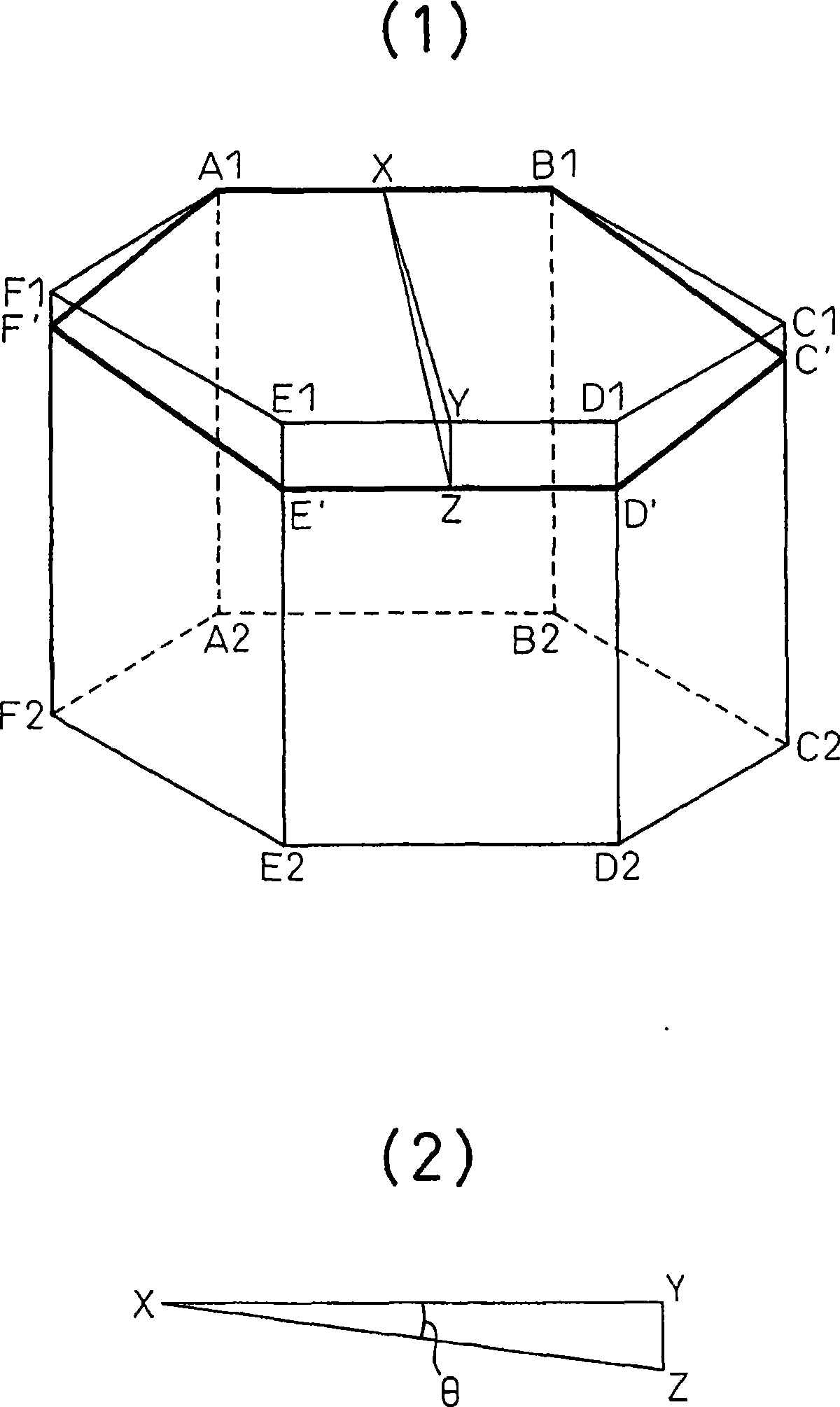
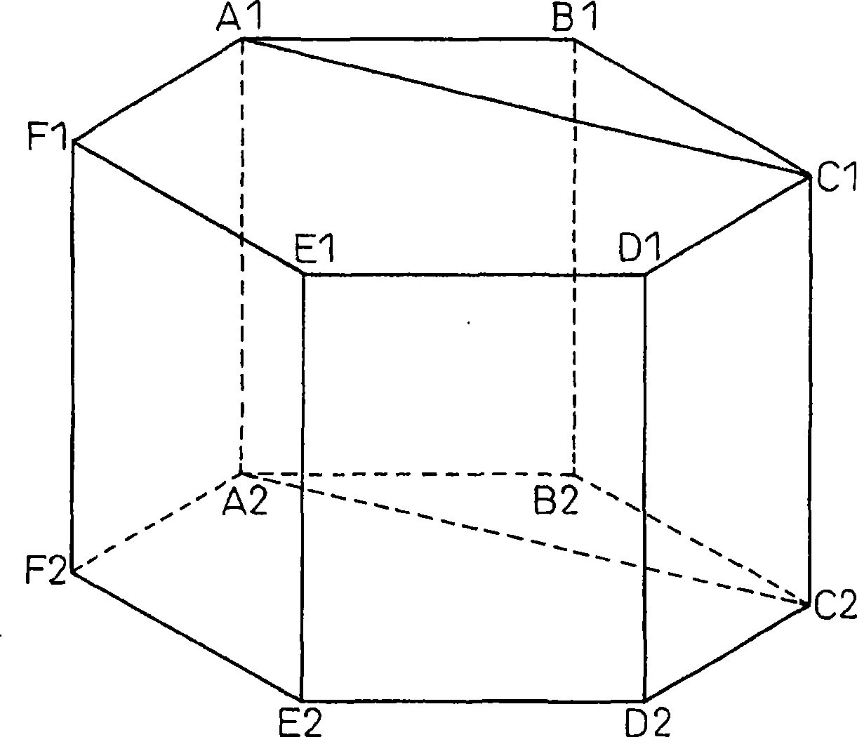
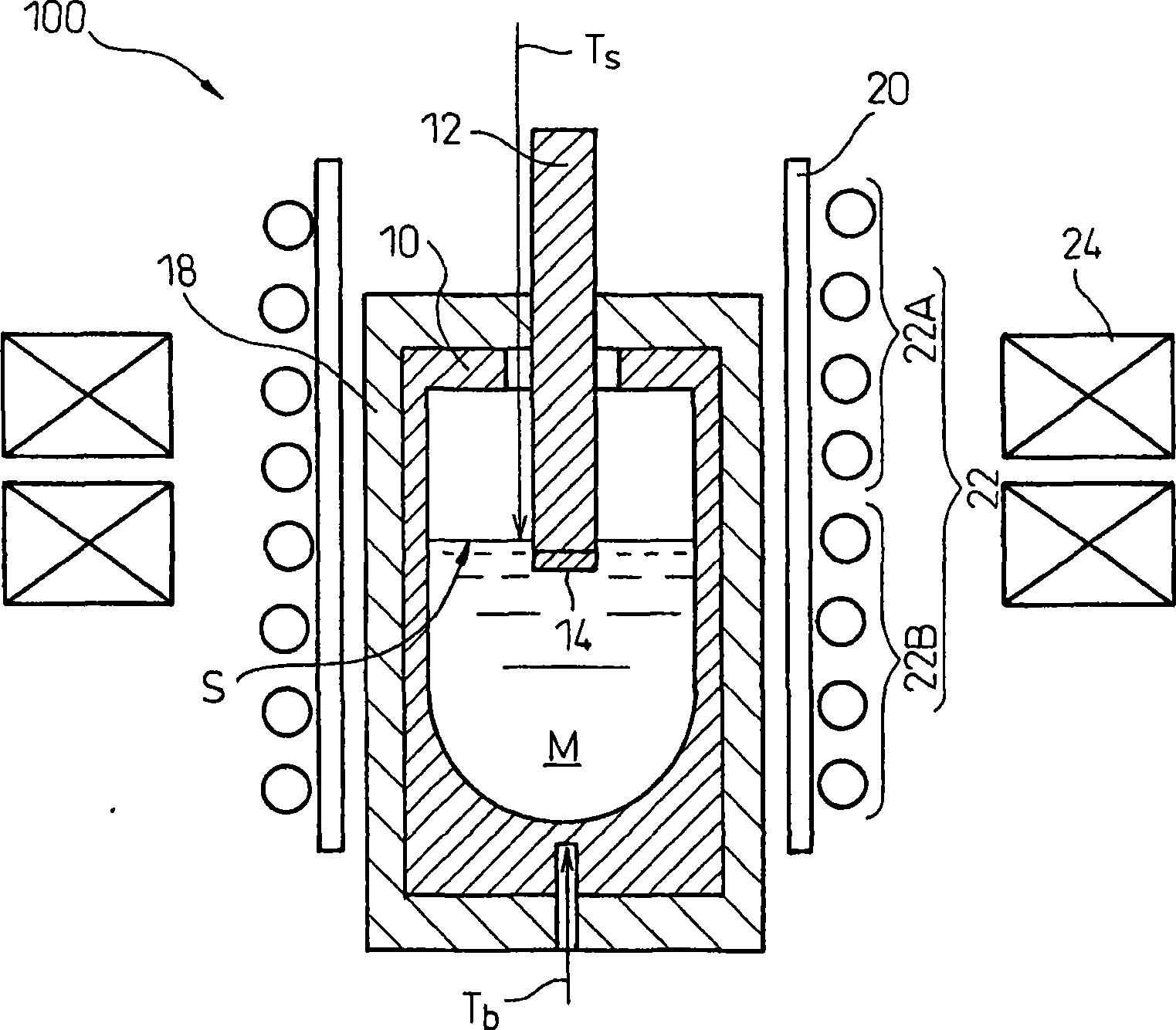
[0039] use image 3 The SiC single crystal production furnace 100 of the present invention is suitable for producing SiC single crystals by the solution method with the deviation angle θ of the present invention.

[0040] In this embodiment, the SiC seed crystal 14 whose growth surface is inclined at an angle of θ=4° relative to the (0001) plane [1-100] direction is installed on the lower end of the graphite rod 12 and inserted into the positive side of the Si melt surface S. Below, a SiC single crystal was grown under the following growth conditions.

[0041] [growth conditions]

[0042] The melt surface temperature Ts of the Si melt temperature is 1800°C, and the temperature gradient from the bottom of the crucible to the melt surface S temperature is set at 20°C / cm. The atmosphere in the crucible is Ar gas and maintained at normal pressure. In order to stabilize the planar growth, Al, which is one of the additive elements already proposed by the present applicant in JP-A...

Embodiment 2

[0045] Install the SiC seed crystal 14 whose growth surface is the (1-100) plane (that is, the deviation angle θ=90° relative to the (0001) direction [1-100] direction) on the lower end of the graphite rod 12, and insert it into the Si melt surface Directly below S, a SiC single crystal was grown under the same growth conditions as in Example 1.

[0046] Figure 5 (1) A photograph showing a section including the growth axis from the graphite rod 12 through the seed crystal 14 to the single crystal growth layer G. SiC single crystals grow with very high planarity on SiC seeds.

[0047] At this time, and then as Figure 5 As shown in the schematic diagram showing the growth surface profile in (2), the diameter of the SiC single crystal grown from the SiC seed crystal (the outline is shown by a dotted rectangle) is approximately doubled or more. There is also a portion where the expansion is terminated due to the multinucleated portion N occurring around a portion, but this ca...


PUM


Abstract

This invention provides a process for producing a SiC single crystal by a solution method, which can stably maintain the flatness of a growth face and can prevent polycrystallization to grow a large-diameter SiC single crystal. The process for producing a SiC single crystal comprises growing a hexagonal SiC single crystal, which starts from a hexagonal SiC seed crystal held just below a melt surface while maintaining such a temperature gradient that the temperature is decreased from the inside of an Si melt within a graphite crucible toward the melt surface. In this process, the SiC single crystal is grown on a plane inclined at a predetermined off angle from (0001) plane of the SiC seed crystal toward (1-100). The off angle is preferably 1 to 30 degrees. Most preferably, the SiC single crystal is grown on (1-100) plane having an off angle of 90 degrees.

Description

technical field [0001] The present invention relates to a method for producing a SiC single crystal by a solution method. Background technique [0002] SiC semiconductors are expected to be used as power devices and environment-resistant devices because they have a larger energy band gap than Si semiconductors and are superior in withstand voltage characteristics, operating temperature, and heat resistance. The crystal system of SiC includes hexagonal crystal, cubic crystal, etc., and 6H type (hexagonal crystal with 6 molecules as one cycle) and 4H type (hexagonal crystal with 4 molecules as one cycle) as semiconductor materials are considered to be effective. Promising, there are various proposals for the production technology of high-grade SiC single crystal suitable for semiconductor materials. [0003] As a method for producing a SiC single crystal, mainly a sublimation method and a solution method are known. The sublimation method is the most common method among SiC s...

Claims


Application Information

Patent Timeline
Patent Type & Authority Applications(China)
IPC IPC(8): C30B29/36C30B19/04
CPCC30B19/04C30B29/36
Inventor 坂元秀光
Owner TOYOTA JIDOSHA KK
Why Eureka
Try Eureka