

Integrated circuit suitable for various encapsulation modes
A technology of integrated circuits and packaging modes, which is applied in the field of integrated circuits with various packaging modes, and can solve the problems that the development and production costs of microchips cannot be effectively saved.
- Summary
- Abstract
- Description
- Claims
- Application Information
AI Technical Summary
Problems solved by technology
Method used
Image

Examples
Embodiment Construction
[0133] Specific embodiments are given below to describe the content of the present invention in detail, and the accompanying drawings are used as auxiliary descriptions. The symbols mentioned in the description are reference figures.
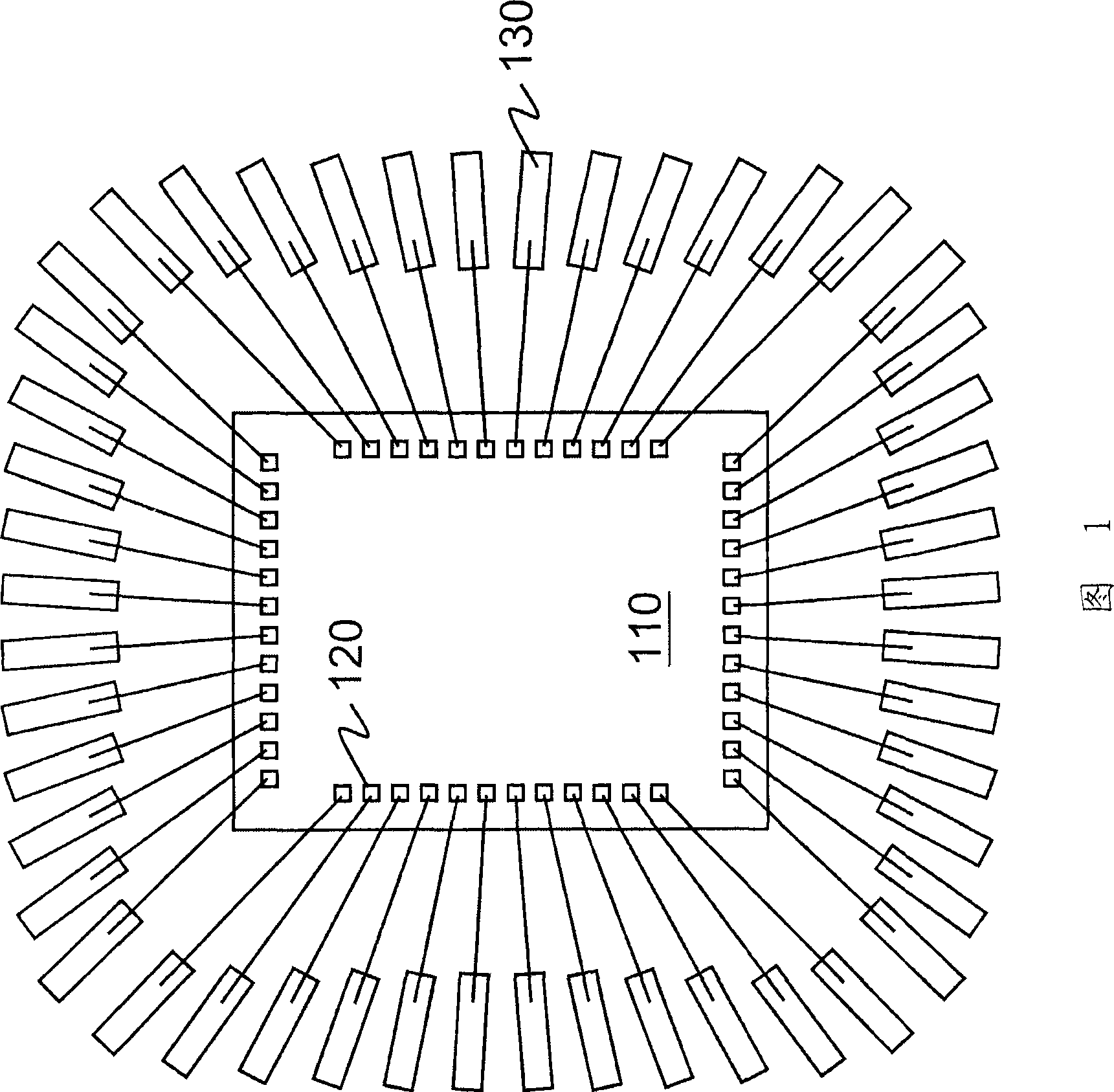
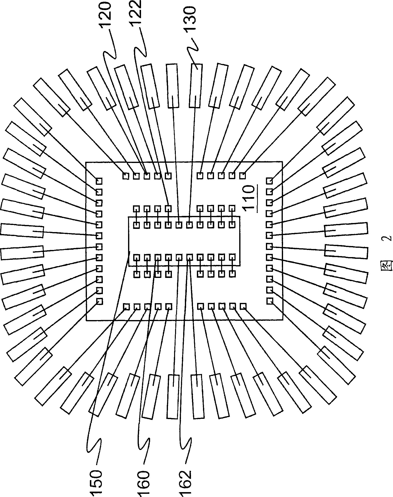
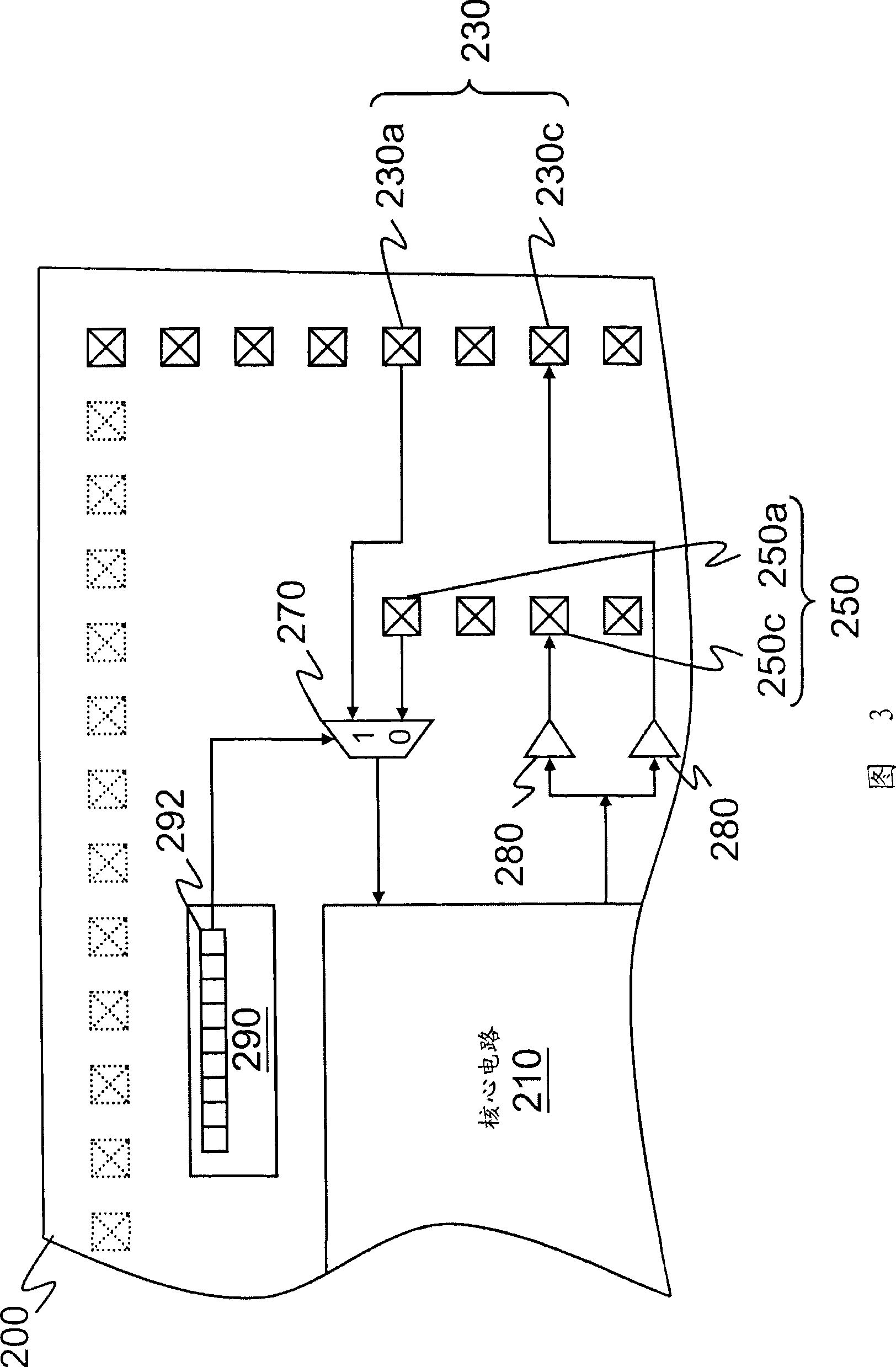
[0134] Referring to FIG. 3 , it is an integrated circuit 200 according to an embodiment of the present invention, which is applicable to various types of packaging, such as single microchip packaging, multi-microchip packaging, and the like. The integrated circuit 200 includes: a core circuit 210 , a plurality of bonding pads 230 , 250 , a selection circuit 270 and a control circuit 290 .
[0135] Here, the core circuit 210 refers to the circuit part used to provide the main core functions of the integrated circuit. Generally speaking, the core circuit 210 will have one or more signal input / output signals. In this embodiment, in order to be applicable to various packaging modes, the signal input terminal is coupled to the selection circuit 270,...
PUM
 Abstract
Description
Claims
Application Information