Light source deviceLight source die set and method for manufacturing the light source device

A technology of a light source device and a light source module, which is applied in the manufacture of semiconductor/solid-state devices, electrical components, electric solid-state devices, etc., can solve the problems of limited application fields and small irradiation range of the light source device 10, and achieve a large irradiation range and simple manufacturing process Effect

Inactive Publication Date: 2009-06-24
FOXSEMICON INTEGRATED TECHNOLOGY (SHANGHAI) INC +1
View PDF0 Cites 12 Cited by
  • Summary
  • Abstract
  • Description
  • Claims
  • Application Information

AI Technical Summary

Problems solved by technology

The light emitted by the light-emitting diode chip 12 can only exit through the hemispherical light-emitting surface 131, that is, it can only exit in a single direction opposite to the light-emitting diode chip 12. Therefore, the irradiation range of the light source device 10 is small, which limits its Application field

Method used


Image

  • Light source deviceLight source die set and method for manufacturing the light source device
  • Light source deviceLight source die set and method for manufacturing the light source device
  • Light source deviceLight source die set and method for manufacturing the light source device

Examples


Embodiment Construction

[0019] The present invention will be further described in detail below in conjunction with the accompanying drawings.

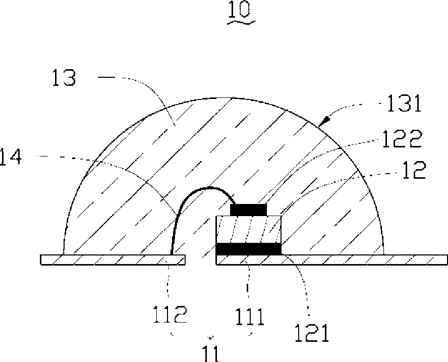
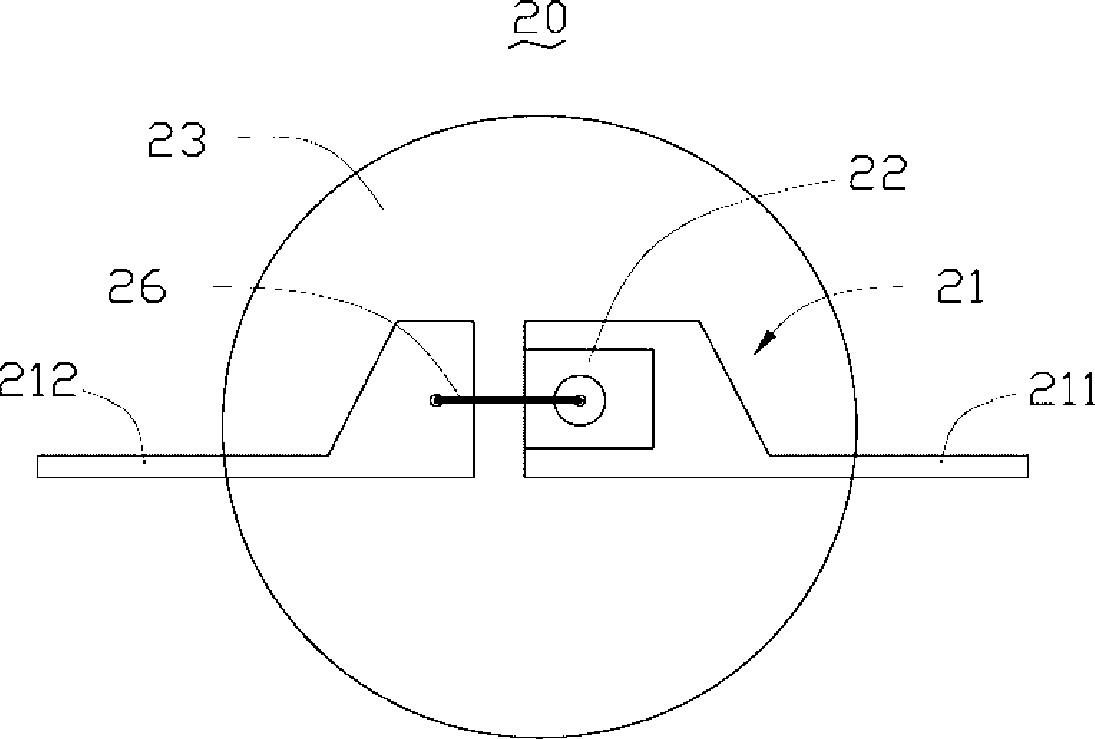
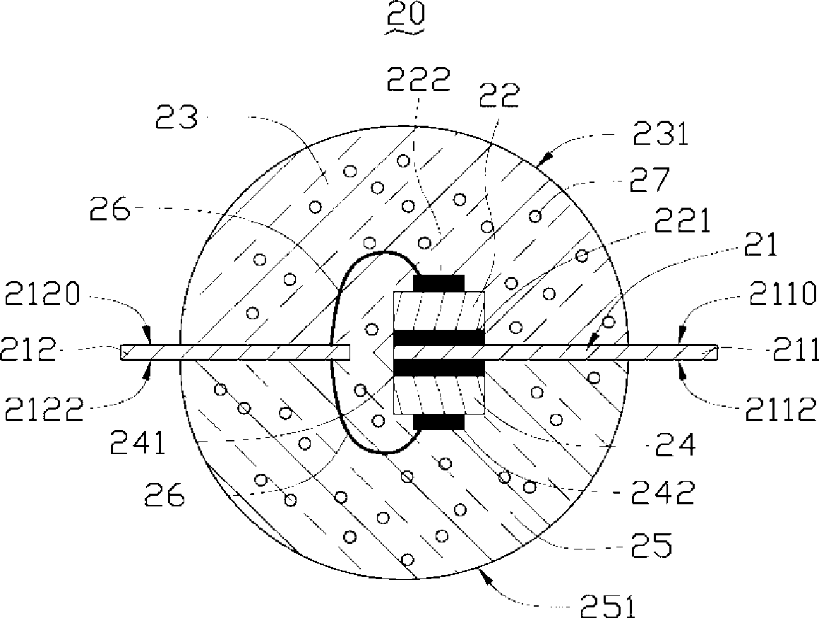
[0020] See figure 2 and image 3 The light source device 20 provided by the first embodiment of the present invention includes a conductive frame 21 , a first solid state light emitting chip 22 , a first package 23 , a second solid state light emitting chip 24 and a second package 25 . The following will be described by taking the first solid-state light-emitting chip 22 and the second solid-state light-emitting chip 24 as light-emitting diode chips as an example.

[0021] The conductive frame 21 includes a first electrode 211 and a second electrode 212 . The first electrode 211 and the second electrode 212 are used for connecting with an external power source. The first electrode 211 includes a first surface 2110 and a second surface 2112 opposite to the first surface 2110, the second electrode 212 includes a first surface 2120 and a second surface 2122,...


PUM


Abstract

The invention provides a method for manufacturing a light source device, which comprises the following steps of providing a conductive bracket; arranging a first solid-state light-emitting chip at one side of the conductive bracket and electrically connecting the first solid-state light-emitting chip with the conductive bracket; forming a first packaging body on the first solid-state light-emitting chip; providing a bearing platform provided with an accommodating groove; placing the first packaging body in the accommodating groove of the bearing platform; arranging a second solid-state light-emitting chip at the other side of the conductive bracket and connecting the second solid-state light-emitting chip with the conductive bracket in a routing manner; forming a second packaging body on the second solid-state light-emitting chip to form the light source device; and disassembling the light source device from the bearing platform. The light source device is a three-dimensional light source and has a larger radiation range.

Description

technical field [0001] The invention relates to a light source device, a light source module and a manufacturing method of the light source device. Background technique [0002] At present, Light Emitting Diode (LED), as a solid-state light-emitting element, gradually replaces Cold Cathode Fluorescent Lamp (CCFL) due to its good light quality (that is, the spectrum output by the light source) and high luminous efficiency. As the light-emitting element of the lighting device, for details, please refer to the article "Solid-State Lighting: Toward Superior Illumination" published by Michael S. Shur et al. in the document Proceedings of the IEEE, Vol.93, No.10 (October 2005). [0003] See figure 1 , an existing light source device 10, which includes a conductive frame 11, a light emitting diode chip 12 and a packaging body 13. The conductive frame 11 includes a first electrode 111 and a second electrode 112, the LED chip 12 includes a first contact electrode 121 and a second c...

Claims


Application Information

Patent Timeline
Patent Type & Authority Applications(China)
IPC IPC(8): H01L25/00H01L25/075H01L23/488H01L23/31H01L21/50H01L21/56H01L21/60
CPCH01L25/075H01L33/54H01L2924/01019H01L2933/0091H01L2224/45144H01L2924/01079H01L33/62H01L2924/01012H01L2224/48091H01L2224/73265H01L2924/00014H01L2924/00
Inventor 赖志铭李泽安
Owner FOXSEMICON INTEGRATED TECHNOLOGY (SHANGHAI) INC
Why Eureka
Try Eureka