MOSFET having a high stress in the channel region and fabricating method thereof

A region and drain region technology, applied in semiconductor/solid-state device manufacturing, semiconductor devices, electrical components, etc., can solve problems such as small process windows, achieve good etching profile, reduce barrier reduction, and improve etching uniformity

Inactive Publication Date: 2009-07-15
INT BUSINESS MASCH CORP
View PDF0 Cites 16 Cited by
  • Summary
  • Abstract
  • Description
  • Claims
  • Application Information

AI Technical Summary

Problems solved by technology

Another typical problem of currently known etching techniques is the loading effect, where the etch profile depends on the pattern density, i.e. the local area density of the etchable material
A third typical problem is that the etch profile of an isotropic or anisotropic recess etch can include crystalline facets that form on the surface of the recessed region, which creates challenges for the subsequent epitaxial growth of the embedded material
Further, the reactive ion etching process described above may have a very small process window

Method used


Image

  • MOSFET having a high stress in the channel region and fabricating method thereof
  • MOSFET having a high stress in the channel region and fabricating method thereof
  • MOSFET having a high stress in the channel region and fabricating method thereof

Examples


Embodiment Construction

[0075] (0038) As noted above, the present invention relates to stressed CMOS devices having stress-inducing materials embedded in source and drain extension regions and methods of fabrication thereof, thereby enabling heterojunctions and p-n junctions between two semiconductor materials Coincidentally, it will be described in detail with reference to the accompanying drawings. It should be noted that identical and corresponding elements are marked with the same reference numerals.

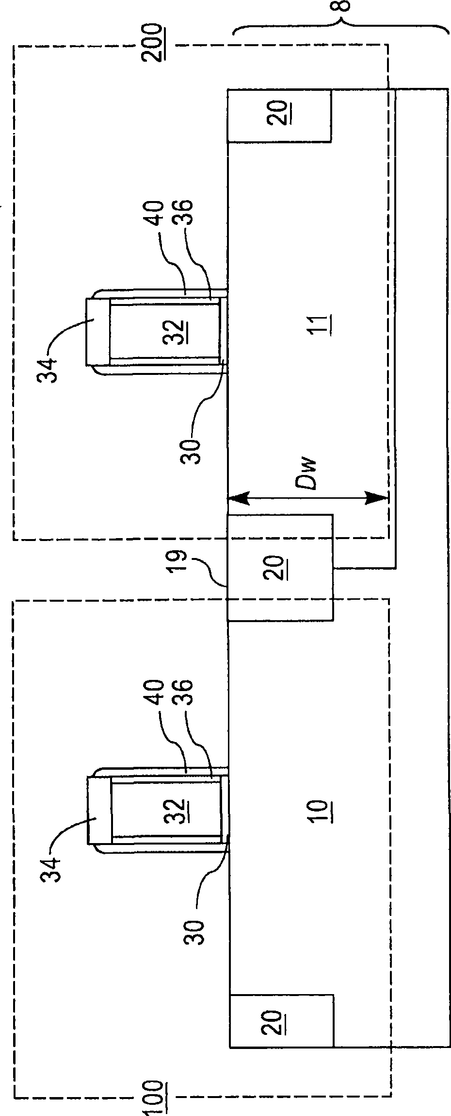
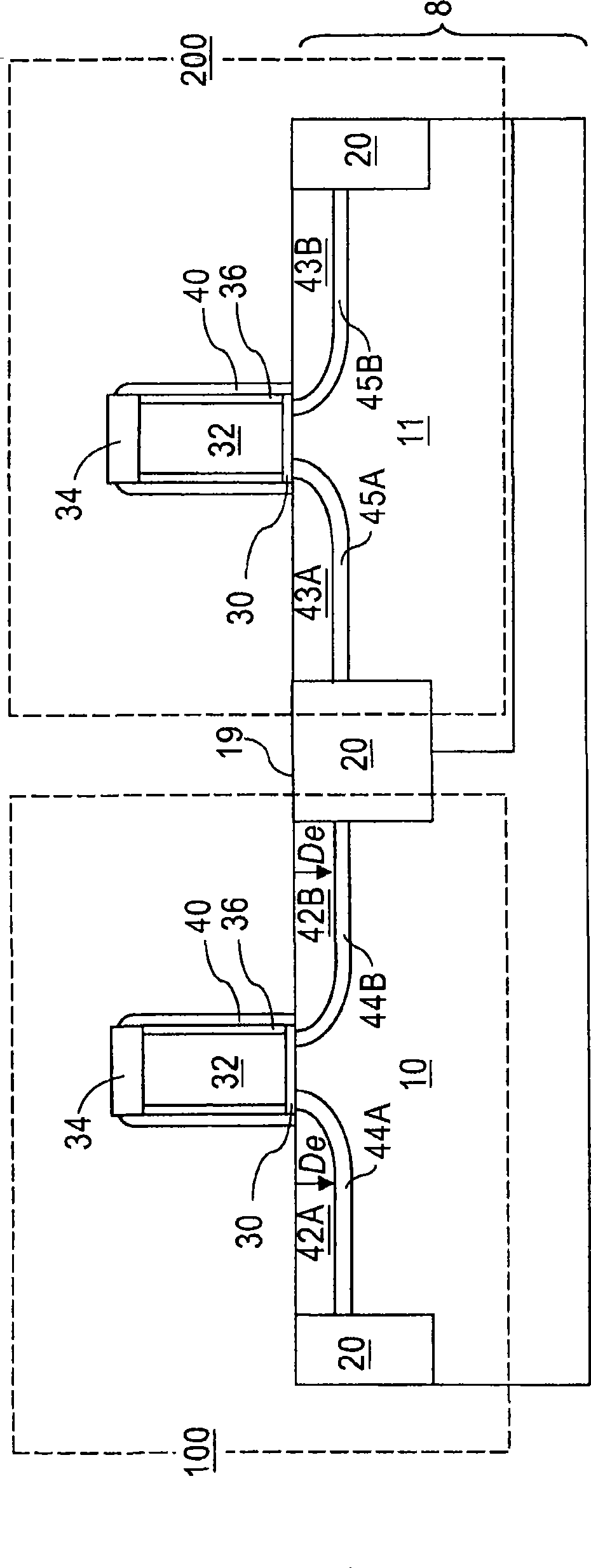
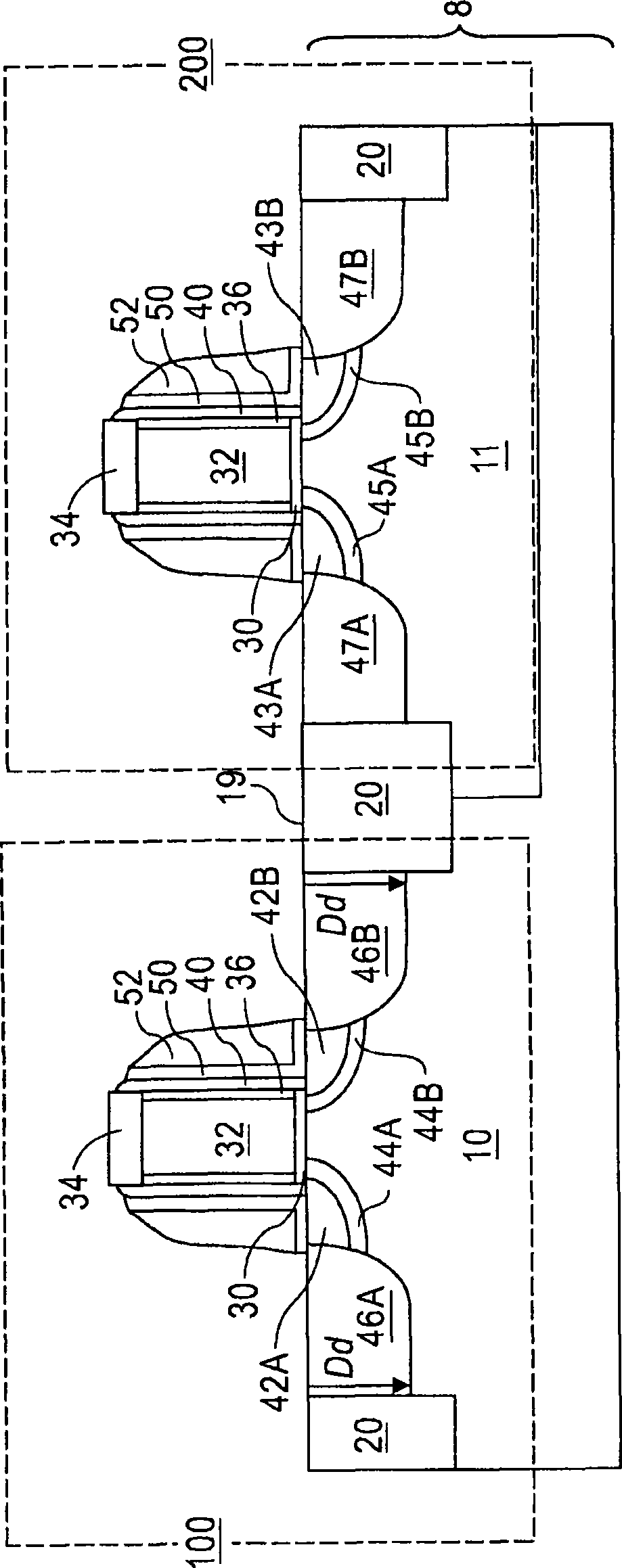
[0076] (0039) Reference figure 1 , shows a first exemplary semiconductor structure according to the first embodiment of the present invention, which includes a semiconductor substrate 8 including a first semiconductor region 10 and a shallow trench isolation 20 . The first semiconductor region 10 comprises a first semiconductor material having a doping of the first conductivity type with a first dopant concentration. The semiconductor substrate 8 may further comprise a second semiconductor regio...


PUM

PropertyMeasurementUnit
thicknessaaaaaaaaaa
thicknessaaaaaaaaaa
thicknessaaaaaaaaaa

Abstract

Source and drain extension regions are selectively removed by a dopant concentration dependent etch or a doping type dependent etch, and an embedded stress-generating material such as SiGe alloy or a Si:C alloy in the source and drain extension regions is grown on a semiconductor substrate. The embedded stress-generating material may be grown only in the source and drain extension regions, or in the source and drain extension regions and in deep source and drain regions. In one embodiment, an etch process that removes doped semiconductor regions of one conductivity type selective to doped semiconductor regions of another conductivity type may be employed. In another embodiment, a dopant concentration dependent etch process that removes doped semiconductor regions irrespective of the conductivity type selective to undoped semiconductor regions may be employed.

Description

technical field [0001] (0001) The present invention relates to high performance semiconductor devices for digital or analog applications, and more particularly to complementary metal oxide semiconductor (CMOS) devices with stress-induced mobility enhancement. Specifically, the present invention provides stressed CMOS devices having embedded stress-inducing materials in source and drain extension regions extending from deep source and drain regions toward the channel and methods of manufacturing the same. The direction protrudes laterally, whereby the heterojunction between the two semiconductor materials coincides with the p-n junction, or is located close to the p-n junction. Background technique [0002] (0002) Various techniques for improving the performance of semiconductor devices by controlling carrier mobility have been studied in the semiconductor industry. A key element in this technology classification is the control of stress in the channel of transistor devices....

Claims


Application Information

Patent Timeline
Patent Type & Authority Applications(China)
IPC IPC(8): H01L29/78H01L27/092H01L21/336H01L21/8238
CPCH01L21/823807H01L29/7833H01L21/823814H01L29/66537H01L29/7848H01L29/66636H01L29/165H01L29/6659H01L29/6656H01L29/6653H01L29/66545
Inventor 欧阳齐庆K·T·肖宁伯格J·耶茨三世
Owner INT BUSINESS MASCH CORP
Why Eureka
Try Eureka