Conductive wire type semiconductor device and conductive wire rack thereof

A semiconductor and lead frame technology, applied in the field of semiconductor devices, can solve problems such as unpredictable circuit system behavior, uneven current distribution, and unsatisfactory segmentation

Active Publication Date: 2009-07-22
SILICONWARE PRECISION IND CO LTD
View PDF7 Cites 0 Cited by
  • Summary
  • Abstract
  • Description
  • Claims
  • Application Information

AI Technical Summary

Problems solved by technology

[0007] Traditionally, in order to simplify the problem, the power supply and grounding are usually treated as an ideal situation, but in high-speed design, this simplification will make it more and more difficult to predict the behavior of the circuit system after implementation
Although the directly visible result of the circuit design is expressed from the signal integrity, the design of the power integrity must not be ignored because the power integrity will eventually be reflected in the signal integrity after being damaged, and in many In most cases, the main cause of signal distortion and disturbance is the power system, for example: unsatisfactory division of multiple power supply / ground planes, too much ground bounce noise, uneven current distribution, etc.

Method used


Image

  • Conductive wire type semiconductor device and conductive wire rack thereof
  • Conductive wire type semiconductor device and conductive wire rack thereof
  • Conductive wire type semiconductor device and conductive wire rack thereof

Examples


Embodiment Construction

[0044] The implementation of the present invention is described below through specific examples, and those skilled in the art can easily understand other advantages and effects of the present invention from the content disclosed in this specification.

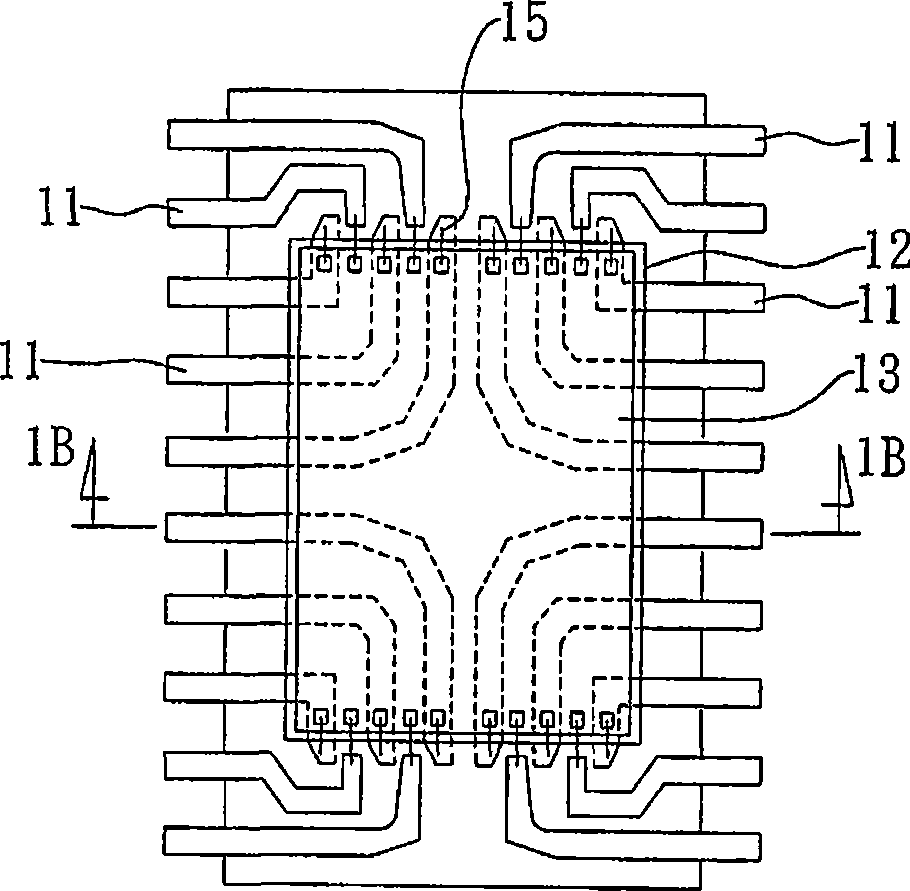
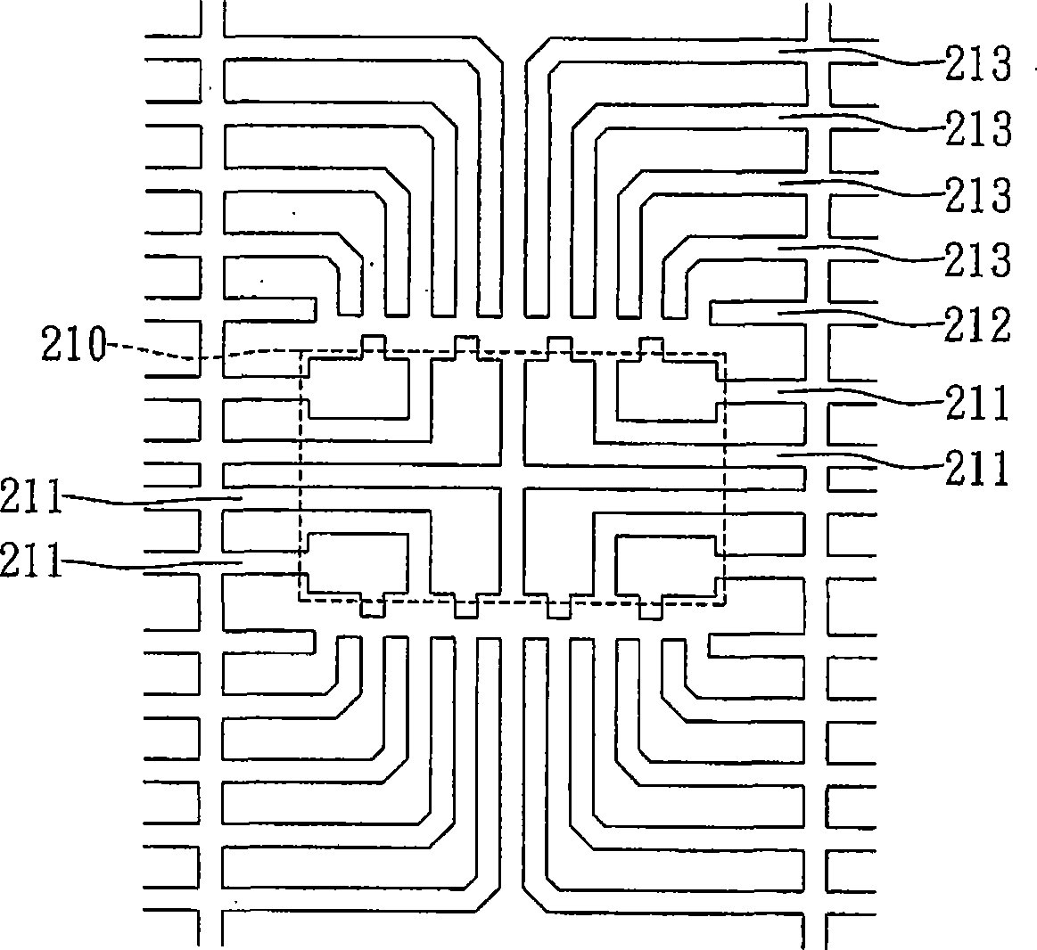
[0045] see figure 2 , is a schematic plan view of the lead frame of the present invention.

[0046] The lead frame includes a plurality of grounding pins 211, and the grounding pins 211 together form a chip placement area 210; a plurality of signal pins 213 are distributed around the chip placement area 210; and a plurality of power supply pins 212 , distributed around the chip mounting area 210 , and the size of the ground pin 211 in the chip mounting area 210 is larger than the size of the signal pin 213 and the power pin 212 .

[0047] That is, the ground pin 211 and the power pin 212 are set relatively independently to improve the ground bounce problem and strengthen the electrical function. The dimensions of the signal ...


PUM


Abstract

The invention discloses a lead frame type semiconductor device and the lead frame thereof. The lead frame which comprises a plurality of signal pins, a plurality of ground pins and a plurality of power supply pins is provided; a plurality of ground pins (or power supply pins) form a chip connecting zone while the other signal pins and power supply pins (or ground pins) are distributed around the chip connecting zone; therefore, the ground pins or the power supply pins are isolated, thus improving the problem of ground bounce and reinforcing electrical property; meanwhile the size of the ground pins (or power supply pins) in the chip connecting zone is larger than the size of the signal pins and the power supply pins (or ground pins) around the chip connecting area, thus a semiconductor chip on the chip connecting zone can have good heat radiation function.

Description

technical field [0001] The invention relates to a semiconductor device, in particular to a lead frame type semiconductor device and its lead frame. Background technique [0002] Traditional lead frame (Lead Frame) type semiconductor packages, as disclosed in patents such as US Pat. lead frame, and stick a chip on the chip holder, then electrically connect the electrode pads (Electrode Pads) on the surface of the chip to the corresponding pins through a plurality of welding wires, and then cover the chip with an encapsulant and bonding wires to form a lead frame semiconductor package. [0003] However, when the above-mentioned traditional lead frame structure design corresponds to the electrical requirements of various chips with different functions and functions, the space for flexible adjustment of the lead layout of the lead frame is really limited, especially for highly integrated and light and thin devices. For chips, the required pin spacing and package size are getti...

Claims


Application Information

Patent Timeline
Patent Type & Authority Applications(China)
IPC IPC(8): H01L25/00H01L23/488H01L23/495
CPCH01L2224/48091H01L2224/48247H01L2924/00014
Inventor 赖雅怡邱淑枝
Owner SILICONWARE PRECISION IND CO LTD
Why Eureka
Try Eureka