Pattern structure of circuit board
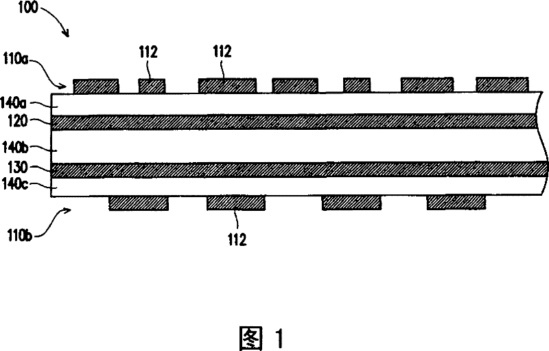
A patterning, circuit board technology, applied in the directions of printed circuit components, electrical components, magnetic/electric field shielding, etc., can solve the problems of increasing the area of the circuit board 100 and the difficulty of wiring the circuit board 100, so as to meet the needs of diversified products Effect
- Summary
- Abstract
- Description
- Claims
- Application Information
AI Technical Summary
Problems solved by technology
Method used
Image
Examples
Embodiment Construction
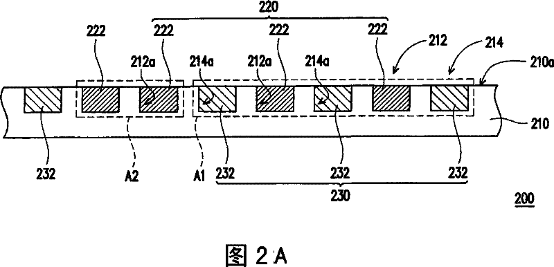
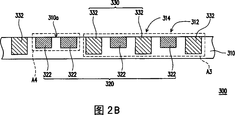
[0043] Figure 2A is a schematic cross-sectional view of a patterned structure of a circuit board according to an embodiment of the present invention, Figure 2B to Figure 2D All are schematic cross-sectional views of patterned structures of circuit boards in other different embodiments of the present invention. It should be explained in advance that the patterned structure of the circuit board of the present invention can be one layer of circuit structure of a multilayer circuit board with two layers, three layers, four layers or more than four layers, and Figure 2A to Figure 2D The patterned structure of the circuit board can be used as the outermost circuit of the circuit board or the circuit structure of any layer inside the circuit board.
[0044] In detail, the circuit board can choose to complete the patterned structure of the present invention as the outermost circuit layer by layer-up method, stacking method or other methods after the inner layer circuit process is ...
PUM
 Abstract
Description
Claims
Application Information


