Silicon thin-film solar cell

A technology of solar cells and silicon thin films, applied in circuits, electrical components, photovoltaic power generation, etc.

Inactive Publication Date: 2009-08-05
CONTREL TECH CO LTD
View PDF0 Cites 5 Cited by
  • Summary
  • Abstract
  • Description
  • Claims
  • Application Information

AI Technical Summary

Problems solved by technology

[0005] However, in the past, there is no multi-level silicon-based thin fil

Method used


Image

  • Silicon thin-film solar cell
  • Silicon thin-film solar cell
  • Silicon thin-film solar cell

Examples


Embodiment Construction

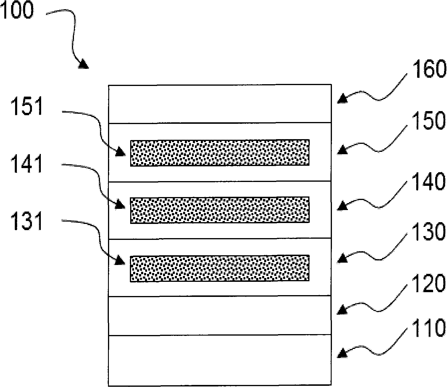
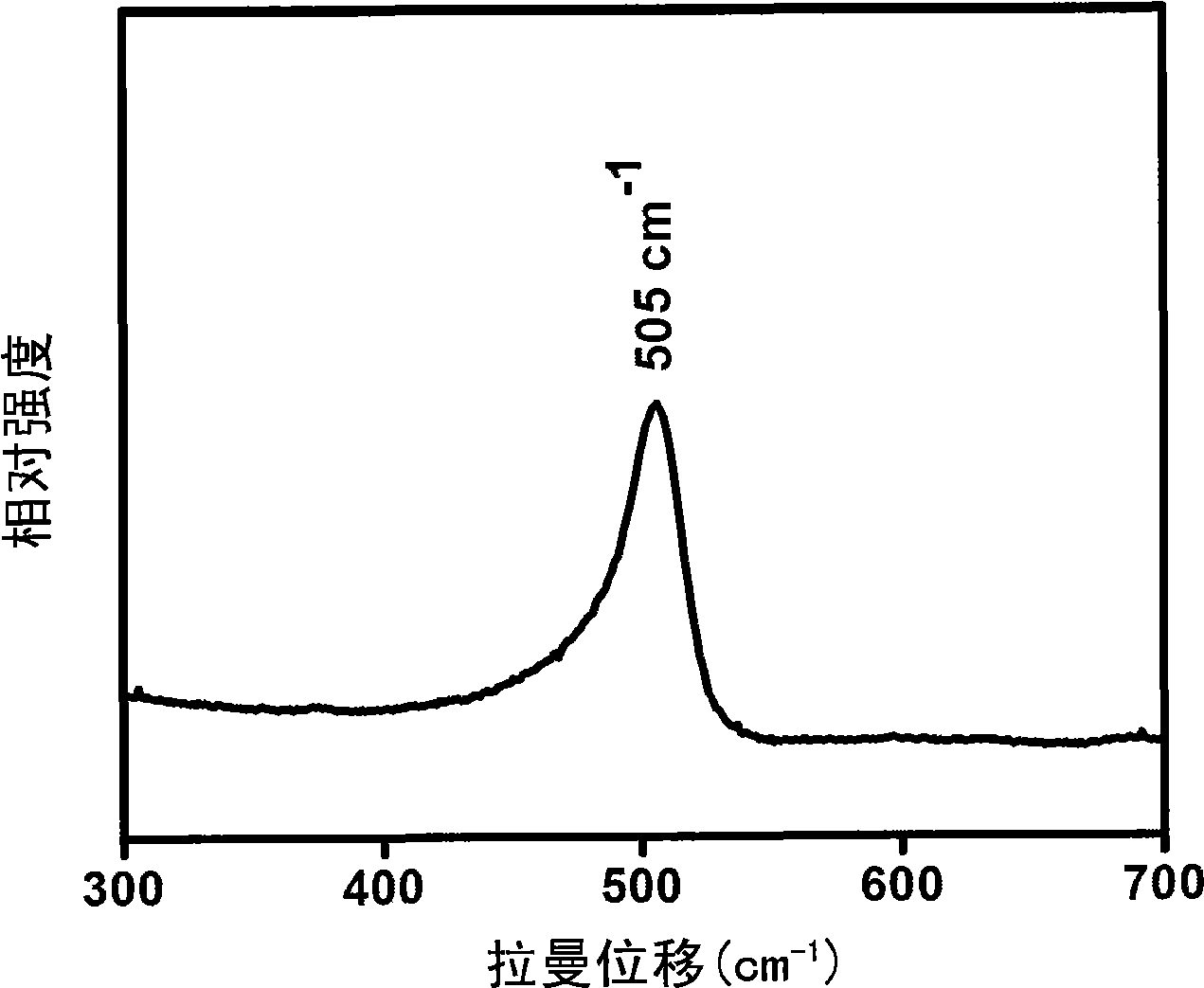
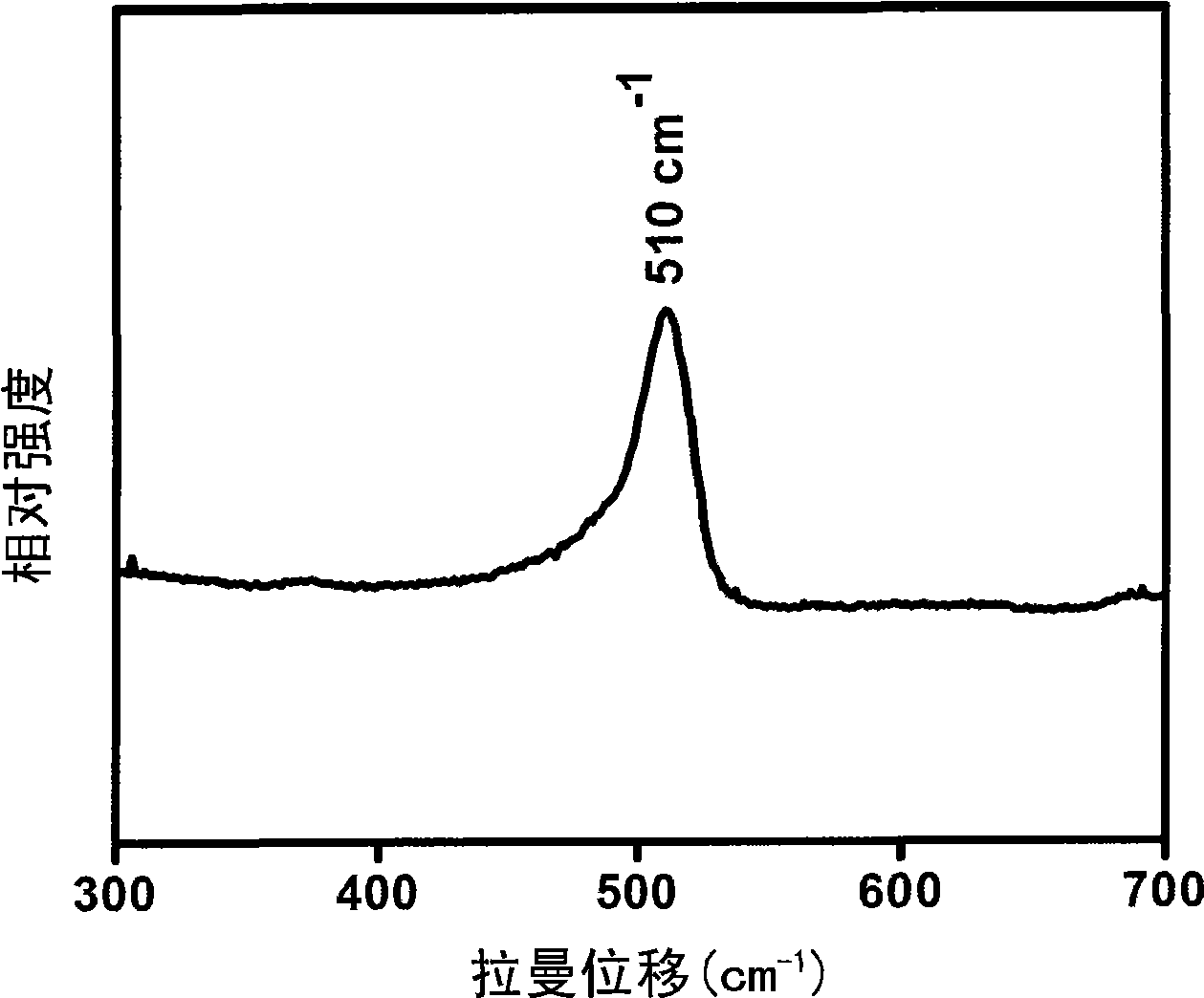
[0028] Please refer to figure 1 , which shows a side cross-sectional view of a silicon thin film solar cell 100, which is the first embodiment of the present invention. The silicon thin film solar cell 100 includes a substrate 110 ; a transparent conductive film 120 ; a P-type semiconductor layer 130 ; an intrinsic (i-type) semiconductor layer 140 ; ​​an N-type semiconductor layer 150 and an electrode 160 . The P-type semiconductor layer 130 has embedded nanocrystalline silicon 131 , the intrinsic (i-type) semiconductor layer 140 has embedded microcrystalline silicon 141 , and the N-type semiconductor layer 150 has embedded polysilicon 151 .

[0029] Since silicon (Silicon) is the representative of the raw materials of solar cells currently in use, it is further divided into: 1. Single crystal silicon; 2. Polycrystalline silicon; 3. Amorphous silicon. At present, the most mature industrial manufacturing technology and the largest market share are photovoltaic panels based on ...


PUM

PropertyMeasurementUnit
Thicknessaaaaaaaaaa
Crystal sizeaaaaaaaaaa

Abstract

The invention relates to a silicon thin film solar cell which mainly includes a substrate, a transparent conductive film, a P-typed semiconductor layer, an intrinsic (i type) semiconductor layer, an N-typed semiconductor layer and an electrode, wherein, in a P-i-N semiconductor layer, different crystal structures are arranged, and the wavelength absorption range of the overall light and the photovoltaic conversion efficiency of the solar cell can be improved.

Description

technical field [0001] The invention relates to a silicon thin-film solar cell, in particular to a P-i-N semiconductor layer with different crystal structures to achieve different energy gap sizes, so as to increase the wavelength absorption range of light. Background technique [0002] At present, due to the international energy shortage, countries around the world have been continuously researching and developing various feasible alternative energy sources. Among them, solar cells for solar power generation have attracted the most attention. Solar cells are easy to use, inexhaustible, inexhaustible, and waste-free. , no pollution, no rotating parts, no noise, can block radiant heat, long service life, size can be changed at will, combined with buildings and popularized, so the use of solar cells as energy is a way to obtain Very efficient form of energy harvesting. [0003] In the 1970s, silicon solar cells first developed by Bell Laboratories in the United States gradual...

Claims


Application Information

Patent Timeline
IPC IPC(8): H01L31/075H01L31/036H01L31/077
CPCY02E10/50Y02E10/547
Inventor 简永杰杨茹媛张育绮田伟辰
Owner CONTREL TECH CO LTD
Why Eureka
Try Eureka