Diode with low frequency, low noise and low twinkling
A low-noise, diode technology, applied in the field of diodes, can solve the problems of overcurrent, too fast reverse recovery time, unstable waveform, etc.
- Summary
- Abstract
- Description
- Claims
- Application Information
AI Technical Summary
Problems solved by technology
Method used
Image
Examples
Embodiment Construction
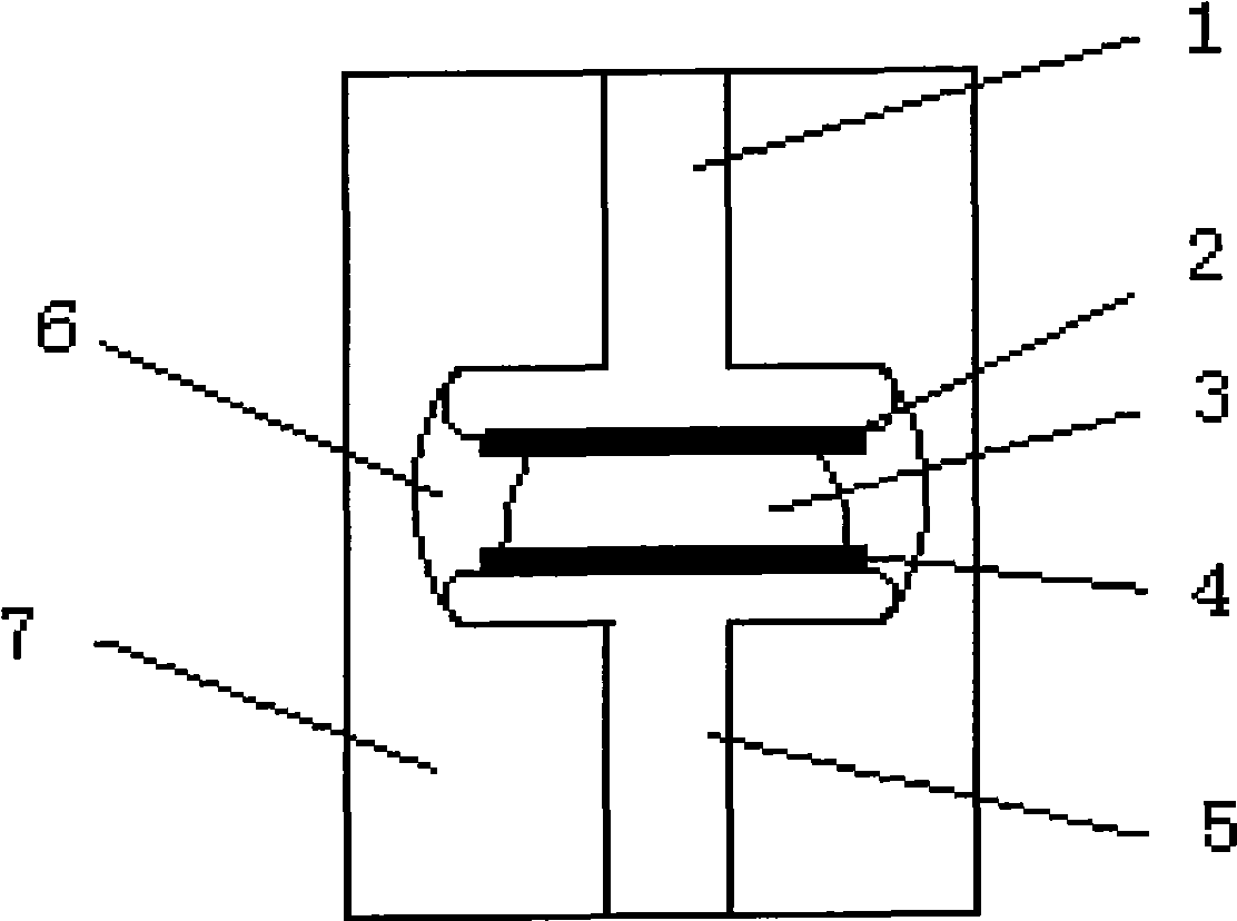
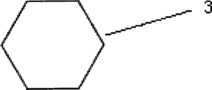
[0008] Such as figure 1 As shown, the diode of the present invention is sequentially welded together by electrode 1, soldering tab 2, chip 3, soldering tab 4, and electrode 5, and is sealed with silicon rubber or polyimide glue 6 between the two electrodes after welding. In order to achieve the purpose of increasing the working current, the chip is designed as a hexagon, such as figure 2 As shown, the maximum opposite surface is 65mil, and the diagonal is 1.91mm; the thickness of the hexagonal chip is 300±5μm; the size of the electrode large table is: 1.92±0.05mm.
[0009] The above components are welded together, and then sealed and connected with a 2.0-2.7mm package 7 to form a complete diode. Because the diode breaks through the traditional shape and size design of electrodes, pads, and chip components, it can pass a working current of 1-2.5A, and has the characteristics of low frequency, low noise, and low flicker.
PUM
 Abstract
Description
Claims
Application Information

