Touch control panel device

A touch panel and insulating layer technology, which is applied in the fields of instruments, electrical digital data processing, electrical components, etc., can solve the problems of noise formation, low production yield, interference with contact point detection, etc.

Inactive Publication Date: 2009-09-30
ELAN MICROELECTRONICS CORPORATION
View PDF0 Cites 26 Cited by
  • Summary
  • Abstract
  • Description
  • Claims
  • Application Information

AI Technical Summary

Problems solved by technology

[0004] However, in the manufacturing process of the above-mentioned capacitive touch panel device, the first extension line unit 16 and the second extension line unit 17 need to be bonded respectively around the top and bottom surfaces of the substrate 11 and overlap the first and second extension line units. When the second wire units 14, 15 are used to electrically connect the first and second electrode units 12, 13, and when the first and second extension line units 16, 17 extend to the outside around the substrate 11, often due to the first and second extension line The gap between the units 16 and 17 with an indeterminate distance causes noise between the first and second extension line units 16 and 17, which interferes with the detection of contact points and causes a problem of low production yield

Method used


Image

  • Touch control panel device
  • Touch control panel device
  • Touch control panel device

Examples


Embodiment Construction

[0072] In order to further explain the technical means and effects of the present invention to achieve the intended purpose of the invention, the specific implementation, structure, characteristics and effects of the touch panel device proposed according to the present invention will be described below in conjunction with the accompanying drawings and preferred embodiments. , as detailed below.

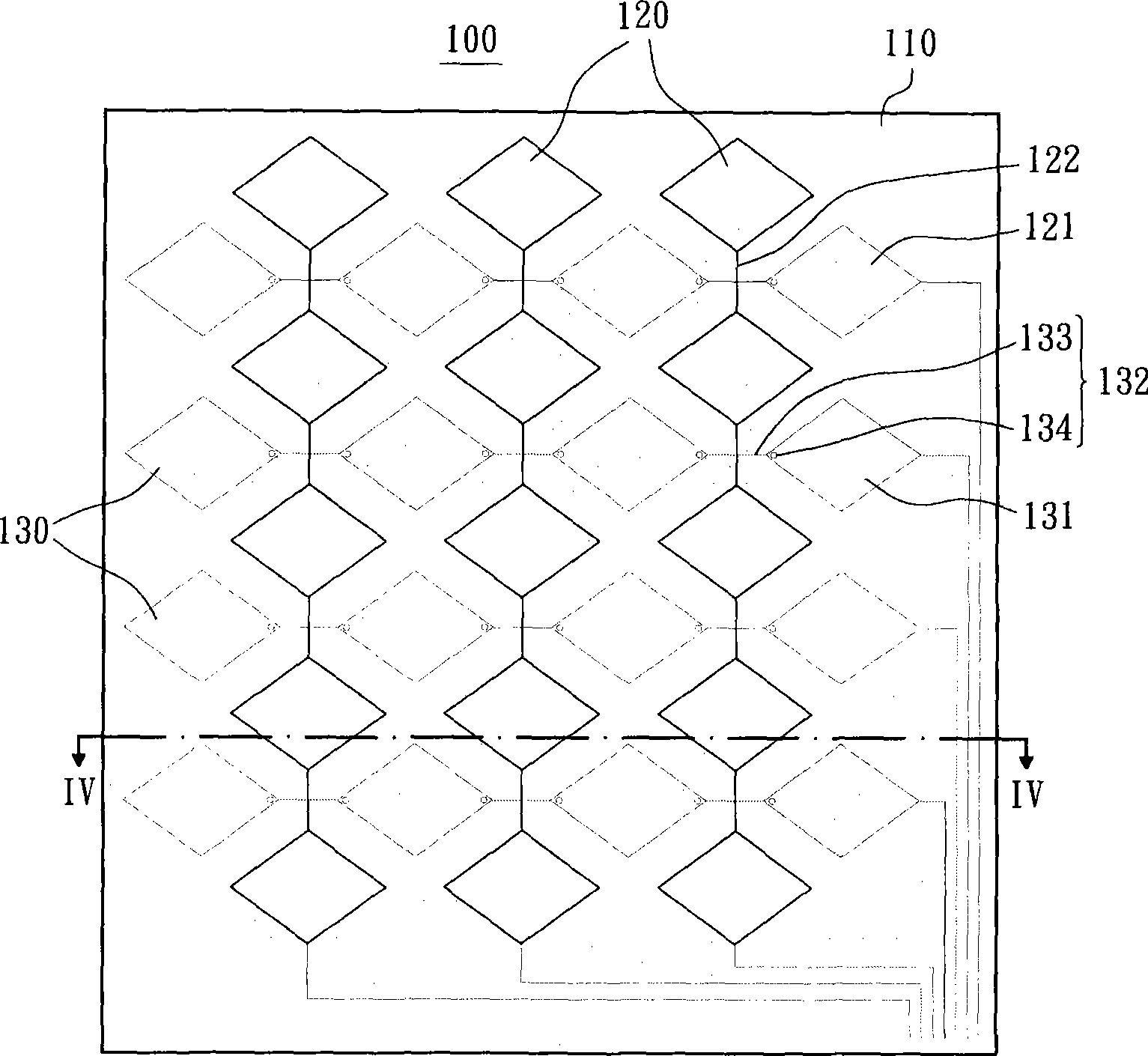
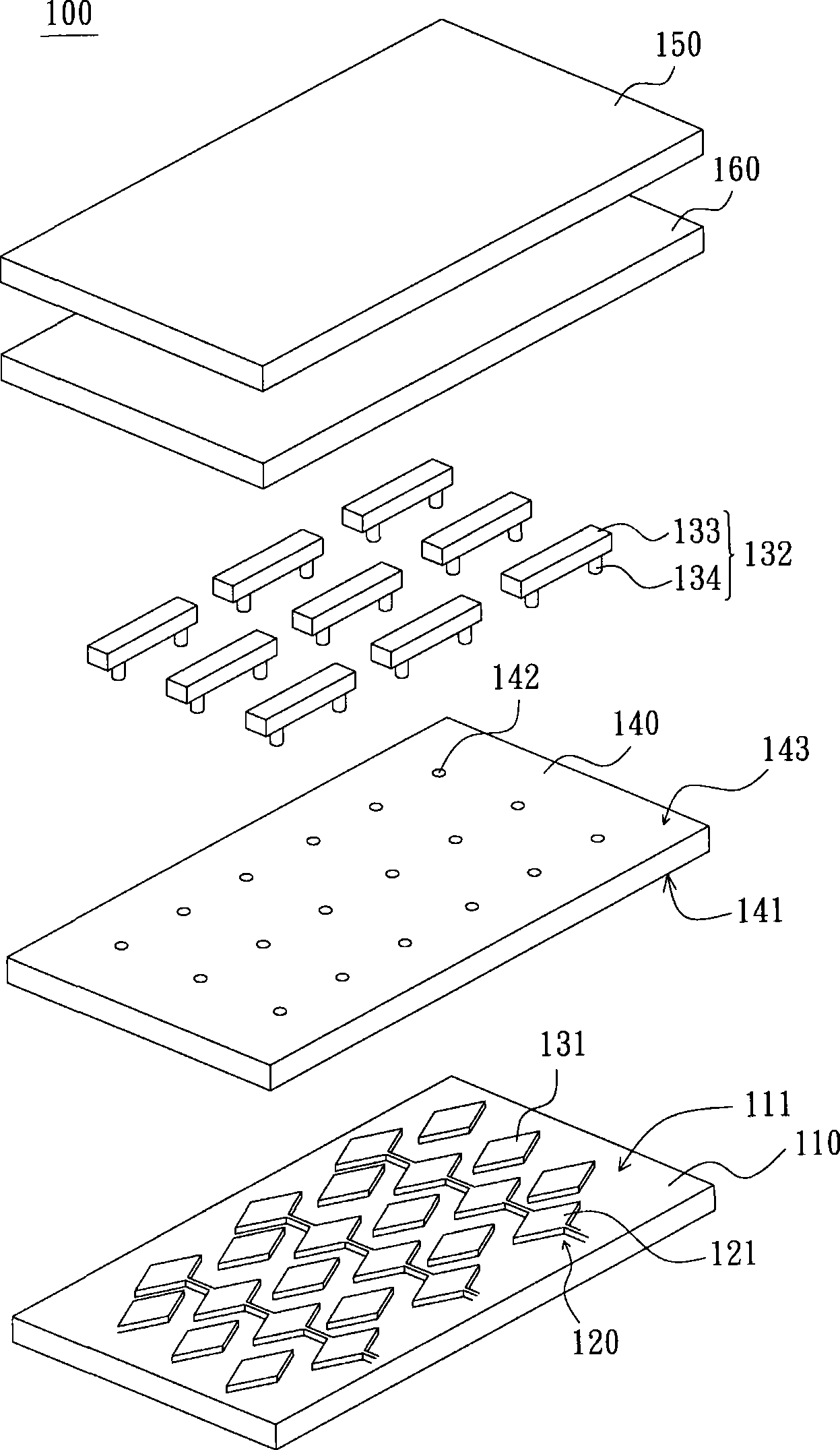
[0073] see Figure 2 to Figure 4 , a touch panel device 100 provided in the first embodiment of the present invention, which includes a substrate layer 110, a plurality of first electrode groups 120, a plurality of second electrode groups 130, an insulating layer 140, an insulating adhesive layer 160 and an anti- The scraping layer 150 ; the substrate layer 110 has a flat surface 111 , which facilitates the formation of the first electrode group 120 and the second electrode group 130 thereon. Here, the first electrode set 120 and the second electrode set 130 can form a capacitive sen...


PUM


Abstract

The invention relates to a touch control panel device, which comprises a base material layer, an insulating layer, a plurality of first electrode groups and a plurality of second electrode groups. The insulating layer is formed on the base material layer and comprises a first surface adjacent to the base material layer and a second surface away from the base material layer. A plurality of first electrode groups are positioned on the first surface of the insulating layer; and each first electrode group comprises a plurality of first electrode pieces which are arranged on the first surface of the insulating layer at intervals and a plurality of first leads which are electrically connected with the adjacent first electrode pieces. Each second electrode group comprises a plurality of second electrode pieces and a plurality of bridging leads which are electrically connected with the adjacent second electrode pieces; a plurality of second electrode pieces are arranged on the first surface of the insulating layer at intervals and are staggered between the first electrode pieces; and the bridging leads are formed on the second surface of the insulating layer. The touch control panel device has a simple structure so as to simplify a manufacturing process and obtain evener sensing sensitivity.

Description

technical field [0001] The present invention relates to a touch panel device, and in particular to a capacitive touch panel device. Background technique [0002] In general life, touch panel devices are widely used in various electronic products, for example, cash machines of financial institutions, navigation information systems of department stores, or personal digital assistants (Personal Digital Assistant, PDA). ) and notebook computers, and can be divided into many different types of touch panel devices according to the different physical principles of detecting touch points. Touch panel devices with different detection principles also have different advantages and disadvantages. [0003] figure 1 Shown is the structure of the current general capacitive touch panel device. This capacitive touch panel device has a flat substrate 11, a first electrode unit 12 formed on the top surface of the substrate 11, and a first electrode unit 12 formed on the bottom surface of the ...

Claims


Application Information

Patent Timeline
Patent Type & Authority Applications(China)
IPC IPC(8): G06F3/044H03K17/96
CPCG06F2203/04111
Inventor 邱延诚
Owner ELAN MICROELECTRONICS CORPORATION
Why Eureka
Try Eureka