FFS type TFT-LCD array substrate structure and manufacture method thereof
A technology of array substrate structure and manufacturing method, applied in semiconductor/solid-state device manufacturing, optics, instruments, etc., can solve problems such as uneven pixel electrode, liquid crystal orientation, confusion, etc., to improve picture quality, eliminate step end difference, and improve freedom degree of effect
Active Publication Date: 2010-12-01
BOE TECH GRP CO LTD +1
View PDF0 Cites 0 Cited by
- Summary
- Abstract
- Description
- Claims
- Application Information
AI Technical Summary
Problems solved by technology
The purpose of the present invention is to provide an FFS type TFT-LCD array substrate structure and its manufacturing method, which can effectively solve the technical defects of the array substrate structure in the prior art, such as disordered liquid crystal orientation caused by uneven pixel electrodes.
Method used
View moreImage
Smart ImageViewing Examples

Examples
Embodiment Construction
Login to View More PUM
 Abstract
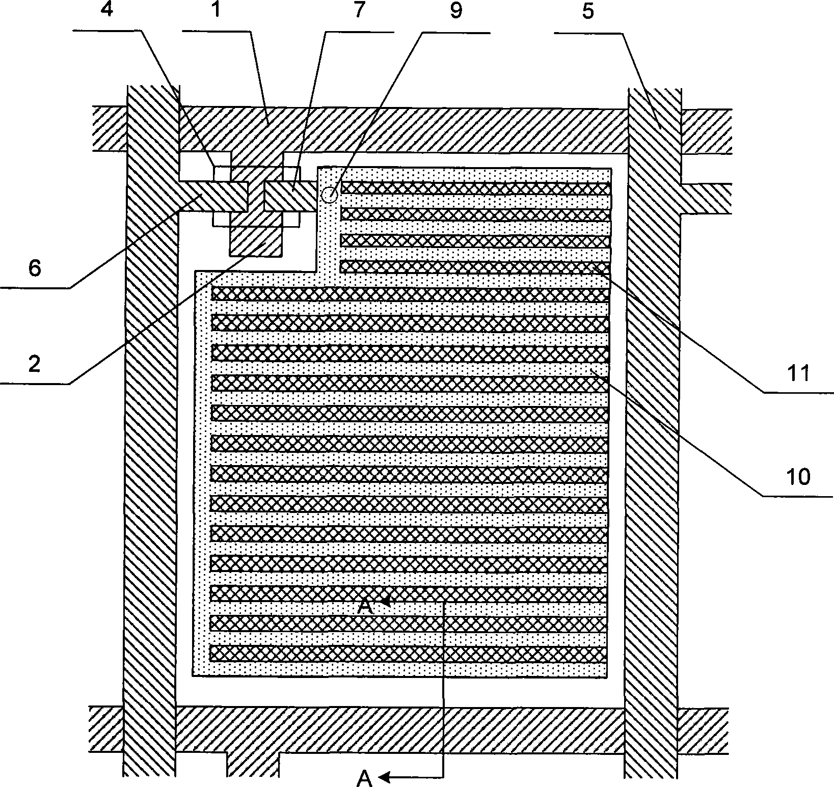
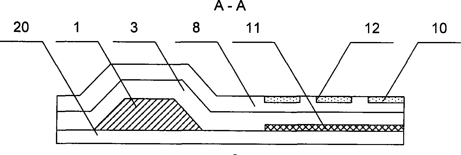
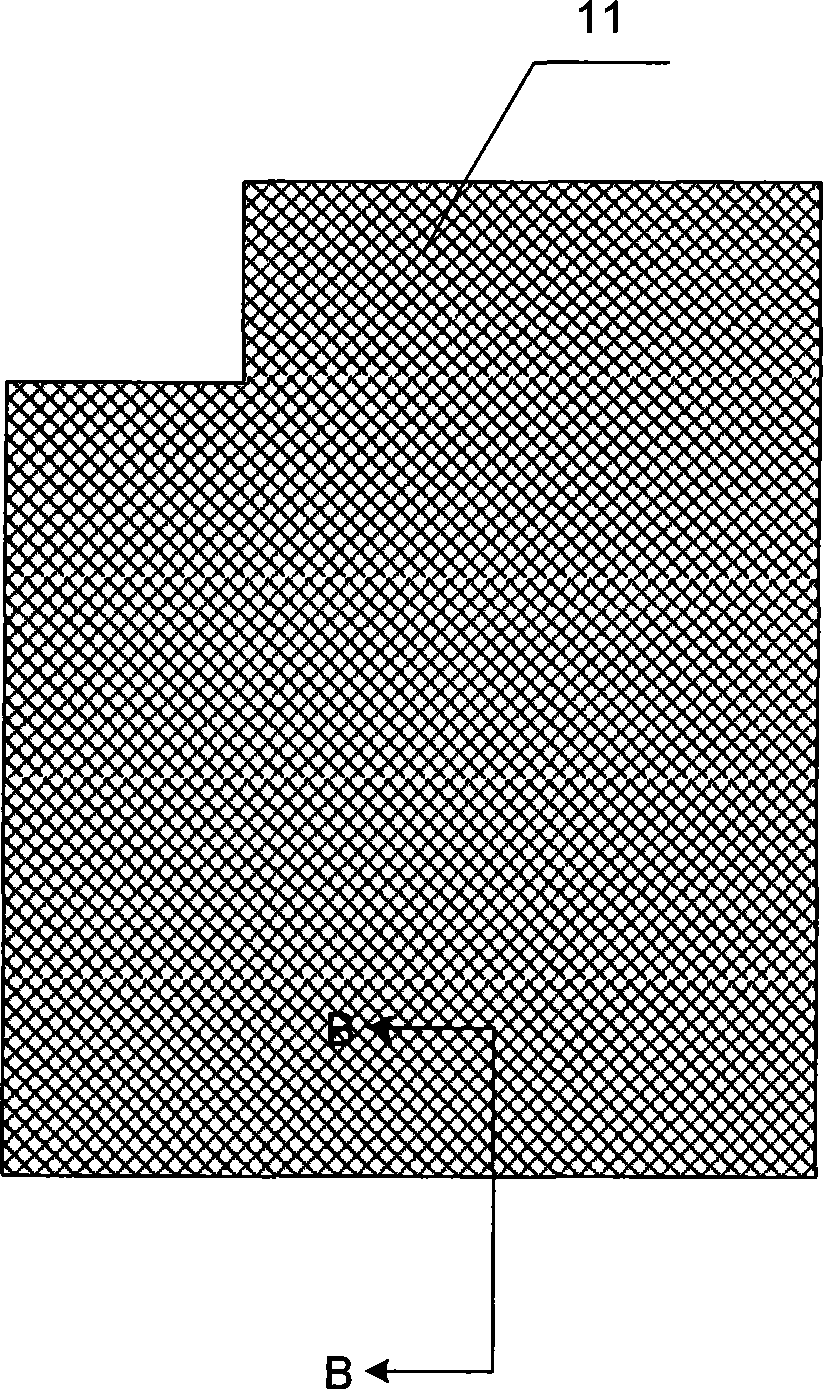
The invention relates to an FFS type TFT-LCD array substrate structure and a manufacture method thereof. The array substrate structure comprises a substrate, a public electrode, a grid line, a grid electrode, a grid insulating layer, an active layer, a data wire, a source electrode, a drain electrode and a passivation layer, wherein the public electrode, the grid line, the grid electrode, the gridinsulating layer, the data wire, the source electrode, the drain electrode and the passivation layer are formed on the substrate; and the active layer is formed on the grid insulating layer and positioned on the grid electrode. Passivation layer grooves which are in strip shapes and are sequentially arranged are formed in a pixel area; a passivation layer through hole is formed at the position ofthe drain electrode; pixel electrodes are formed on the passivation layer, positioned in the passivation layer grooves and connected with the drain electrode through the passivation layer through hole. The invention farthest eliminates the terminal temperature difference (TTD) of the pixel electrodes in the pixel area, and flat surfaces of the pixel electrodes ensure that the subsequent frictionorientation process of orientation films can obtain uniform orientation angles, thereby the quality of pictures is improved, and the degree of freedom for designing the pixel electrodes is greatly improved.
Description
FFS type TFT-LCD array substrate structure and manufacturing method thereof technical field The invention relates to a thin film transistor liquid crystal display and a manufacturing method thereof, in particular to an FFS type TFT-LCD array substrate structure and a manufacturing method thereof. Background technique In recent years, with the popularization of digital TV, the traditional CRT display has been gradually replaced by a new generation of display devices, including PDP, OLED, LCD, etc., among which Thin Film Transistor Liquid Crystal Display (TFT-LCD) has a small size, Features such as low power consumption, no radiation, and high display resolution have begun to be widely popularized and become mainstream products. Fringe Field Switching (FFS for short) is one of the technologies that have emerged in recent years that can improve the image quality of LCDs, and can simultaneously meet the requirements of high penetration and large viewing angles. The so-called ...
Claims
Login to View More Application Information
Patent Timeline
 Patent Type & Authority Patents(China)
IPC IPC(8): G02F1/1362H01L27/12H01L23/522H01L21/84H01L21/768
Inventor 陈旭闵泰烨林承武谢振宇
Owner BOE TECH GRP CO LTD
Features
- R&D
- Intellectual Property
- Life Sciences
- Materials
- Tech Scout
- Unparalleled Data Quality
- Higher Quality Content
- 60% Fewer Hallucinations
Learn More Browse by: Latest US Patents, China's latest patents, Technical Efficacy Thesaurus, Application Domain, Technology Topic, Popular Technical Reports.
© 2025 PatSnap. All rights reserved.Legal|Privacy policy|Modern Slavery Act Transparency Statement|Sitemap|About US| Contact US: help@patsnap.com